
Greg Stitt. Design the Circuit, then Write the Code. StittHub (Jan. 2024). https://stitt-hub.com/design-the-circuit-then-write-the-code/.
@Article{Stitt2024-1,
author = {Stitt, Greg},
journal = {StittHub},
title = {Design the Circuit, then Write the Code},
year = {2024},
month = jan,
note = {\url{https://stitt-hub.com/design-the-circuit-then-write-the-code/}},
}
Target audience: beginning/intermediate hardware designers, junior/senior engineering undergraduates
There is one saying my former students probably got tired of me saying: “design the circuit, then write the code.” In other words, you should know what you want your synthesized circuit to look like before you start writing any code. I would argue it is the most important rule to following when writing register-transfer level (RTL) code.
The idea is somewhat controversial because many people would argue that you should describe code in the way that is most natural to the designer, and then let the RTL synthesis tools optimize it accordingly. Alternatively, I’ve heard people argue that you should “separate function from architecture” by describing the code in a way that is independent (in theory) of any specific circuit implementation. The synthesis tools could then (again, in theory) create an optimized circuit for a given target architecture. While I agree that such a strategy would be ideal, the reality is that RTL synthesis tools will create significantly different circuits for different coding practices, even when those coding practices have similar or even identical simulation behaviors.
This discrepancy arises largely from the fact that RTL code was originally introduced for the purposes of documenting the behavior of hardware via simulation. As such, RTL languages include constructs that only make sense in the context of simulation, and will either not work for synthesis, or will lead to significantly different designs compared to other constructs. Even when only considering the synthesizable constructs of an RTL language, there are still numerous ways to describe a circuit’s behavior so that it either won’t synthesize, or will synthesize into an unintended circuit.
The fundamental problem is that code with similar simulation behaviors can result in different circuits. Therefore, it is critically important to decide what you want your circuit to be, and then write the code that is guaranteed to synthesize into that circuit.
What do I mean by “design the circuit?”
This methodology can be difficult to understand when first starting with RTL code. “Design the circuit” is in fact pretty vague. The basic idea is you need to have a picture (mental or physical) of your design as a schematic consisting of well-understood types of logic (e.g., finite-state machines, controllers, combinational logic, sequential logic, datapaths, pipelines, memories, etc.). I generally consider one of my own circuits “designed” when I can create a schematic of each part of the design hierarchy, where each component in the hierarchy has also been “designed” based on the type of logic. If a component is a pipeline, I always have a schematic with the exact resources, interconnection, and most importantly, the exact number and location of all registers. If it is a finite-state machine, I draw out the states, next-state transitions, and output logic. If it is a datapath, I create a schematic. If it is some variant of a finite-state machine with datapath, I’ll draw out the states, state transitions, and assign datapath operations to specific states. I almost always know the exact number of registers I want before I start writing any code.
Once you have this “design,” writing the corresponding RTL code that synthesizes to exactly what you want is often trivial. In fact, writing the RTL code should be the easy part. It is designing the circuit that requires creativity. In a later post, I will provide links to my VHDL and SystemVerilog tutorials, which teach these languages with this methodology in mind.
Let’s look at a few basic examples of where writing the code before designing the circuit can cause problems.
Example 1: Adding Multiple Numbers
A very common synthesis problem I saw in my classes was for designs that had to add multiple numbers. So, we’ll start with an example circuit that adds eight numbers.
The problem with inexperienced RTL designers is that they’ll recognize functionality that would be trivial in software code, and will immediately jump in and start writing RTL code. For example, they might do something like this in SystemVerilog:
module add1 #(
    parameter int DATA_WIDTH = 16
) (
    input  logic [DATA_WIDTH-1:0] inputs[8],
    output logic [DATA_WIDTH-1:0] sum
);

    always_comb begin
        sum = '0;
        for (int i = 0; i < 8; i++) begin
            sum += inputs[i];
        end
    end

endmodule
While this code will certainly simulate correctly, it will likely not be an attractive solution. As a sanity check for your design, you should always take a look at the schematic after elaboration. Using Vivado, we see something like this:
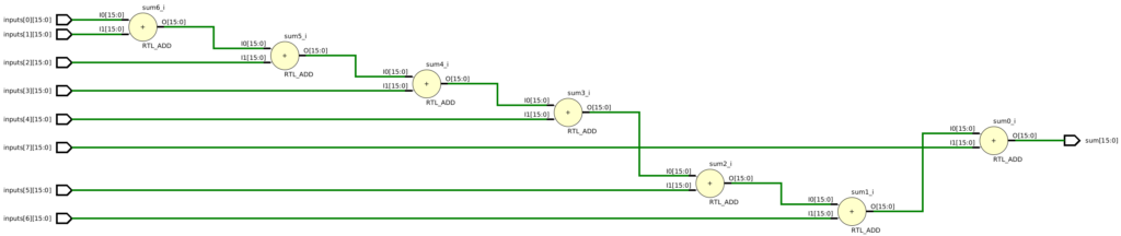
Experienced RTL designers will immediately recognize the potential problem here is that this code synthesizes all the additions as combinational logic, with 7 adders chained together. Although this design could be a good solution for a low clock constraint, it will likely not be effective for high-performance designs due to a lengthy critical path. Synthesis optimizations like tree-height reduction might reduce the maximum path length to 3 adders, but it still likely won’t ever achieve high clock frequencies.
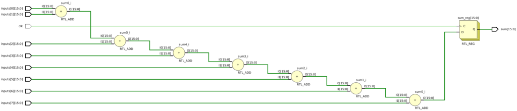
Upon realizing this clock limitation, an inexperienced designer will often recognize they need some registers, and may simply throw the previous loop into a clocked always block:
module add2 #(
    parameter int DATA_WIDTH = 16
) (
    input  logic                  clk,
    input  logic [DATA_WIDTH-1:0] inputs[8],
    output logic [DATA_WIDTH-1:0] sum
);

    always @(posedge clk) begin
        sum = '0;
        for (int i = 0; i < 8; i++) begin
            sum += inputs[i];
        end
    end

endmodule
However, this code has a bunch of problems. First, it breaks the common rule of not using blocking assignments in a clocked process. Second, if there is another clocked process that reads the sum, there will be race conditions because of the blocking assignments. Third, and most relevant to this post, it doesn’t actually add any registers in between the adders:
Again, once an inexperienced designer realizes there are no registers, they might think the problem occurs because they are using blocking assignments, and then do something like the following:
module add3 #(
parameter int DATA_WIDTH = 16
) (
input logic clk,
input logic [DATA_WIDTH-1:0] inputs[8],
output logic [DATA_WIDTH-1:0] sum
);
always_ff @(posedge clk) begin
sum <= '0;
for (int i = 0; i < 8; i++) begin
sum <= inputs[i];
end
end
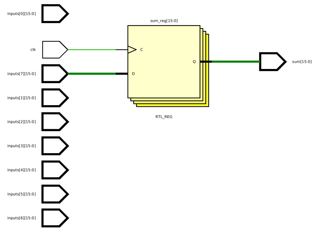
endmoduleHowever, this doesn’t work as intended. In fact, this will synthesize to a single register that assigns the value inputs[7]:
The fundamental problem here is that the inexperienced designer doesn’t have an exact circuit in mind. They have a behavior in mind. They know the behavior should add 8 numbers, but they haven’t thought about how. They then write code hoping that it synthesizes to something correct and efficient. Without an idea of the circuit, and without an understanding of how code synthesizes, that strategy will often run into problems.
How do we avoid these problems? We design the circuit first. What does that mean in this example? Well, before I even create the I/O, I would start asking questions like “how often do inputs arrive, what clock frequency is needed, is there a latency constraint, is there a throughput constraint, is there an area constraint?” Those are questions that need to be answered to fully design the circuit. I can’t write any code for this application yet, because I have no idea what the circuit should look like.
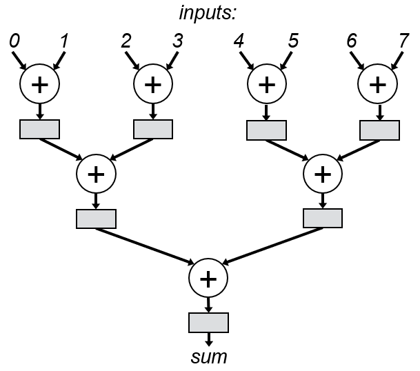
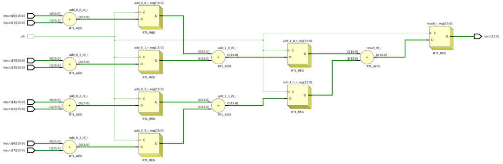
Let’s try to answer some of these questions. Let’s assume a use case that provides 8 inputs potentially every cycle, so we need to be able to output a sum every cycle (after some latency). Let’s assume our optimization goal is to maximize clock frequency, but we also have a latency constraint of 3 cycles to produce an output. We now have some information to work with to design our circuit. The original, pure-combinational logic design, shown in the add1 module, meets our throughput and latency constraint, but is unlikely to maximize clock frequency. So, what we probably want is a pipelined adder tree like the following:
We now have a schematic for a pipeline. In other words, we have designed our circuit. We can now translate that design into code in any way that will synthesize to our schematic. If you don’t know how to write code that synthesizes to a specific circuit, you can follow my tutorials, which will be posted here soon. For simplicity, I’ll use the following behavioral implementation:
module add4 #(
    parameter int DATA_WIDTH = 16
) (
    input  logic                  clk,
    input  logic [DATA_WIDTH-1:0] inputs[8],
    output logic [DATA_WIDTH-1:0] sum
);

    logic [DATA_WIDTH-1:0] add_0_0_r, add_0_1_r, add_0_2_r, add_0_3_r, add_1_0_r, add_1_1_r, result_r;

    always_ff @(posedge clk) begin
        // First row of adders + registers.
        add_0_0_r <= inputs[0] + inputs[1];
        add_0_1_r <= inputs[2] + inputs[3];
        add_0_2_r <= inputs[4] + inputs[5];
        add_0_3_r <= inputs[6] + inputs[7];

        // Second row of adders + registers.
        add_1_0_r <= add_0_0_r + add_0_1_r;
        add_1_1_r <= add_0_2_r + add_0_3_r;

        // Final adder + register
        result_r  <= add_1_0_r + add_1_1_r;
    end

    assign sum = result_r;

endmodule
Looking at the Vivado schematic, we have the exact circuit we designed:
Alternatively, maybe a different use case has constraints that allow for an output to be produced every 16 cycles. In this case, the circuit could be optimized to use a single shared adder. We would first create that schematic, and then update the code accordingly.
There are ultimately millions of possible ways of implementing this simple application. By writing code without explicitly deciding what kind of circuit to create, you are basically crossing your fingers and hoping the synthesized design will be efficient. Avoid this mistake by designing the circuit, then writing the code.
Example 2: One-shot Pulse Generation
In the previous example, several of the coding attempts were just bad coding practices. In this new example, we look at an interesting situation where two different sets of code provide the exact same simulation behavior within the set of assumptions for our use case. However, each one synthesizes differently, with one having a potentially dangerous issue.
In this example, we consider applications that have some notion of a go signal that starts a potentially lengthy operation. For example, a GCD calculator might not do anything until the user asserts a go input, at which point it computes a result over some number of cycles that varies based on the inputs.
In many cases, you don’t want a continuously asserted go signal to cause multiple executions of a circuit. For example, if you connect go to a button, you can’t possibly press the button without triggering numerous executions.
To deal with this issue, you could build logic into a finite-state machine that requires go to be cleared before re-executing. This strategy is simple, but I don’t often use it because it complicates good assertion-based testbench design, and can increase the number of states and logic.
Instead, I often use a separate circuit that generates a single 1-cycle pulse when there is a rising edge on the go signal. This ensures that if go is asserted indefinitely, only one execution will occur. This logic is often referred to as a “one-shot” pulse generator, although that term is broader than our specific purpose here. We’ll now look at two ways of creating this one-shot pulse generator. We’ll make the simplifying assumption that the input trigger is synchronized with the clock.
First, let’s consider a potential mistake inexperienced designers could make. Like before, they try to capture the desired behavior without thinking of the implications of synthesis. Their code might look something like this:
module one_shot1 (
    input  logic clk,
    input  logic rst,
    input  logic in,
    output logic out
);

    logic end_pulse;

    always_ff @(posedge in or posedge end_pulse) begin
        if (end_pulse) out <= 1'b0;
        else out <= 1'b1;
    end

    always_ff @(posedge clk or posedge rst) begin
        if (rst) end_pulse <= 1'b1;
        else end_pulse <= out;
    end

endmodule
Basically, they check for a rising edge on the input, and then assert the output. That output remains asserted until the next rising clock edge, at which point the second always block resets the output by asserting the end_pulse signal.
Behaviorally, this code does exactly what we want. However, some weird things happen during synthesis. Let’s look at the schematic from Vivado:
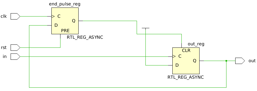
Upon first glance, this schematic looks pretty efficient, and we confirmed the simulation behavior, so it seems like this should work. However, here’s what I typically see next. A person will take this code and use it to trigger another circuit. They synthesize that design, put it on an FPGA, and maybe they get lucky and it works. However, there is a significant problem with this code. At some point, this problem will cause failures on the FPGA, which is what we want to avoid at all costs because it is incredibly hard to debug.
What is the problem here? The problem is that by literally checking the rising edge of the input, that input acts as a clock signal on the right flop (check the schematic closely). When you connect this one-shot to another circuit, that circuit is likely using the actual clock signal. So, what did we just accidentally do? We introduced communication across multiple clock domains. It “works” sometimes for the same reason other multiple clock-domain designs sometimes work: metastability doesn’t always occur. But, it almost certainly will at some point.
How do we fix this design? Well, if we really wanted to use this design, we would have to modify the constraint file to add a clock constraint for the in signal. Without this constraint, the timing analyzer can’t make any guarantees about setup and hold violations for the paths that use the output because it doesn’t know anything about the timing of that output. Assuming the in signal is synchronized to the clock, we could treat it as a generated clock and add a corresponding constraint. That’s a pretty simple fix, but now our code doesn’t work by itself. Without the corresponding constraint file, it will potentially have metastability issues within anything connected to the one-shot. That’s a pretty big annoyance.
Alternatively, we could have avoided this annoyance by following my rule of designing the circuit first. To avoid extra constraints, we want to only use the clock signal on flops. Ultimately, we could just track the previous input every cycle using a single flop, and then assert the output if the previous input is 0 and the current input is 1 (i.e., a rising edge). We can do that with a single flop, an inverter, and an and gate, which will achieve the exact same simulation behavior as the previous example. Our circuit is now designed, so let’s write the corresponding code that will synthesize to that circuit:
module one_shot2 (
    input  logic clk,
    input  logic rst,
    input  logic in,
    output logic out
);

    logic prev_r;

    always_ff @(posedge clk or posedge rst) begin
        if (rst) prev_r <= 1'b0;
        else prev_r <= in;
    end

    assign out = in && !prev_r;

endmodule
As usual, let’s make sure the synthesized circuit matches our design:
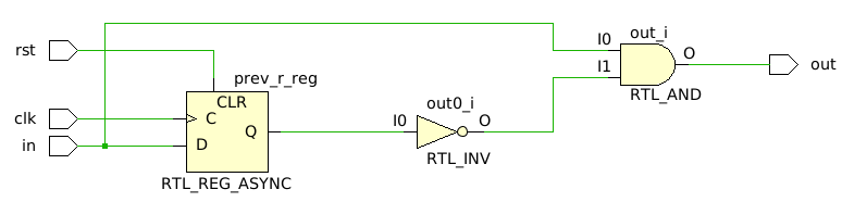
There we go! We now have the exact behavior we want, and a circuit that is efficient and avoids relying on extra constraints for correctness. We were able to accomplish this because we explicitly decided we wanted a flop, an inverter, and an and gate. In other words, we designed the circuit, then wrote the code.
Are there any exceptions to this rule?
The only time I synthesize code without an explicit design in mind is when I want to see how synthesis handles a specific piece of code. For sequential logic, I almost never do this because all of my coding guidelines (see my tutorials) are based on understanding how registers are synthesized and optimized.
However, there are situations where I’m creating complex combinational logic that is more convenient to write as behavioral code than as a complex structural architecture with priority encoders, muxes, etc. While I generally know what will be synthesized based on experience, I don’t always know. Synthesis tools are good at optimizing combinational logic and I’ve run into situations where synthesis optimized my behavioral code more effectively than my structural code.
I don’t view this as an exception to my rule. I see it as an experiment to see if synthesis can perform optimizations that can improve my design. If so, great. If not, it’s doing something differently than the circuit I designed, so I need to revise the code accordingly. However, I always have a design in mind when writing the code.
Summary
A fundamental problem with RTL coding is that different pieces of code can have similar, or even identical, simulation behaviors, but still synthesize to completely different circuits. As such, it is critically important to decide what you want your circuit to look like, and then implement it in a way that will synthesize into that circuit. I refer to this methodology as “design the circuit, then write the code.”
Acknowledgements
This article was created using equipment from University of Florida that was provided via a courtesy appointment.
Updates
1/27/2024: Fixed minor typos.
This reminds me of something I did once that I also think Brian Nezvadovitz did when we were students of yours at different times.
Both of us had some programming experience and realized that verilog/vhdl are somewhat functional programming languages that’s evaluation path results in a synthesis so we implemented the tiered adder you described recursively with an arbitrary procedure (or …something…man it’s been am minute…)
I found it! https://github.com/brandonpollack23/digital_design/blob/c46742022153739fb5bcf45b750f642b634b4617/lab3/turnin/adder_super.vhd#L20
I wonder how you would do this in verilog (its been so long since I’ve done hardware synthesis)
Coincidentally, this is one the articles I’m current working on. I’ve been meaning to add recursive RTL to my tutorial for ages.
Also, I’ll be doing a bunch of VHDL vs SystemVerilog comparisons to highlight the advantages (and annoyances) of each language.
This is great! I remember you first mentioning “design the circut then write the code” to us in the early weeks of Digital Design. I think this is especially valuable for younger engineers in various industries just starting out in creating designs with VHDL or verilog. Very excited to follow where your website goes from here!