
While serving on the banquet panel at the 2024 ACM/SIGDA International Symposium on Field-Programmable Gate Arrays, I was asked “if you could start your career over, what would you work on?” My answer was “I would rebuild FPGA synthesis tools from the ground up.”
When I left academia, this was one of the projects I was working on, but unfortunately couldn’t finish before leaving. Now that I’m in industry, I have an indefinite timeline for finishing it, so I’m passing along my ideas in the hope that I can collaborate with others to fully realize them.
What’s wrong with existing tools?
I’m certainly not alone in my frustrations with FPGA tools. I’ve been publishing in the FPGA community for almost 25 years, and I can’t remember a single conference where tool deficiencies (to put it nicely) were not a common theme. To be fair to tool vendors, FPGA compilation is an incredibly difficult problem. I’ve developed high-level synthesis tools, RTL synthesis tools, placers, routers, and even binary synthesis tools, where I have ultimately repeated nearly all the limitations of existing technologies. However, from this experience, I have come to realize a potential solution to the vast majority of FPGA tool problems, which is the focus of this article.
From my many discussions with other frustrated FPGA designers, I can typically put their complaints into one of three categories:
Category 1: Why isn’t this working? (e.g., tool bugs, inconsistent/incomplete language support, IP problems, vague error messages)
Category 2: Why is this taking so long? (e.g., day-long compilation times)
Category 3: Why can’t the tool do this for me? (e.g., common timing optimizations, design-space exploration)
Category 1 is where tool vendors deserve some blame. FPGA tools have numerous bugs and annoyances that designers have been forced to work around for decades, which I’ll discuss in future articles. Despite Category 1 problems being frustrating, they are rarely the biggest productivity bottleneck in my experience.
If you’ve worked with FPGAs on any reasonable-sized design, you’ve certainly run into Category 2 problems. Unlike software compilation, where most people are used to compilation times on the order of seconds or minutes, FPGA compilation often takes hours, or even days. For most of my designs, I consider myself lucky if I get more than one “turn” (i.e., full compile) per day. For larger designs with tight constraints, 8+ hour compilations are normal. I had one design that took two weeks for a single compilation.
Category 2 is undoubtedly a productivity bottleneck, one that I spent much of my academic career trying to solve (e.g., [1-5]), but if you work with FPGAs long enough, you’ll run into even more annoying problems where you will inevitably ask yourself, “why can’t the tool just do this for me?” These are Category 3 problems.
Category 2 problems unfortunately don’t have an easy solution without sacrificing area or performance. However, even without a solution to Category 2 problems, solving Category 3 problems will significantly improve FPGA productivity. Personally, I wouldn’t care if FPGA compilation took weeks if I could rely on it to solve all the problems I have to solve manually.
Examples of Category 3 problems
In this section, I’ll describe some simple examples of the Category 3 problems I deal with almost daily. We’ll then discuss how to automate solutions to these problems.
Example 1: balancing pipelining delays
The vast majority of high-performance designs I create utilize pipelining. While pipelines are conceptually simple, there are some RTL annoyances that have likely led everyone at some point to ask why the tool can’t handle these annoyances automatically.
Let’s consider the example dataflow graph shown below:
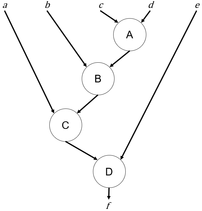
I’ve purposely left the graph abstract because the same annoyance exists regardless of whether each node is a bit-level operation, an arithmetic operation, or a high-level task.
Although a thorough discussion of all pipelining considerations is beyond the scope of this article, a pipeline will generally add some number of registers to each node to improve throughput and/or clock frequency. Pipelines ideally take new inputs every cycle, or more generally every x cycles. This amount of time in between inputs is called the initiation interval, which for simplicity we’ll assume is one in the examples.
For the pipeline to work correctly, we must delay the edges in the graph to ensure that inputs arrive at each node at the same time, as shown below:
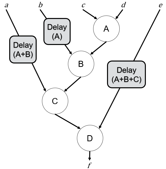
For example, input b needs to be delayed by the latency of A, input a must be delayed by the sum of the latencies of A and B, and input e must be delayed by the sum of the latencies of A, B, and C.
Let’s look at a more specific example, where we assign each node a specific floating-point arithmetic operation with different latencies:
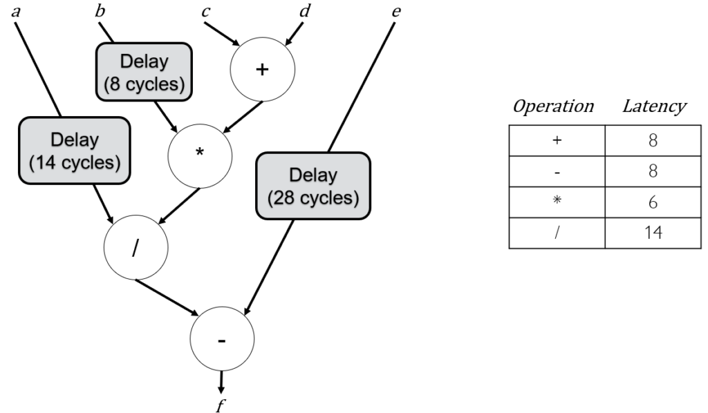
In this example, the b input is delayed 8 cycles (the latency of the add), input a is delayed by 14 cycles (the latency of the add and multiply), and e is delayed by the 28 cycles (the latency of the add, multiply, and divide).
Although this example is relatively easy to implement, for complicated examples, I’ve spent numerous hours figuring out correct delay values that can range from 1 to 100s of cycles in different places. In some cases, I’ve had to make complicated spreadsheets, which inevitably leads to mistakes that are challenging to identify in simulations. Even worse, if I later change the latency in one place, I have to account for that change in many places, which is error prone. Finally, I’ll often make the amount of pipeline stages in each node parameterized, which means I can’t just hardcode the delays. They have to be calculated, which leads to further annoyances when various mathematical exceptions occur.
In addition, the challenge isn’t simply aligning delays, but deciding on the types of resources to use for delays. Above some depth, it might become more efficient to use RAM resources instead of registers. But, which RAM resources? Based on the width and depth of the delay, it makes sense to choose different types of on-chip RAM. Furthermore, you might need a combination of resources. Let’s say we have a delay of 513 cycles, and have an on-chip RAM resource that is 512-words deep. If we use two RAM instances, we utilize barely 50% of those resources, so it might make more sense to instantiate a RAM for 512 cycles and then use flip flops for the final cycle. Furthermore, for course-grain tasks, it might be more efficient to replace the delays with FIFOs.
For a complex enough example, the seemingly simple problem of how to delay edges in a graph becomes a massive design-space exploration problem that is begging to be automated.
Example 2: timing optimization
While I don’t know what percentage of my time is spent doing timing optimization, I can confidently say the vast majority of my tool frustrations occur here. Many FPGA engineers I’ve talked to go as far as reconsidering their career choice due to these frustrations.
While obvious timing bottlenecks are usually reasonably easy to solve, at some point you’ll reach the challenging situation where you optimize a path, which changes the placement of the design to create a new bottleneck. You’ll then optimize the new bottleneck and see a new failing path. After repeating this process numerous times, you’ll eventually realize you haven’t actually accomplished anything other than shifting the original timing bottleneck somewhere else. This infamously frustrating process has many names, but my favorite is timing-optimization “whac-a-mole” (credit to Konboyé Oyake), where each time you “whack” one path, a new failing path pops up. In my opinion, timing optimization is the Category 3 problem that would dramatically improve FPGA productivity if automated. Currently, there are few designers that can solve these types of timing optimization problems, largely because it requires a massive amount of perseverance (some might say craziness) and expertise to escape the whac-a-mole loop.
Let’s look at a few simple, but very common, timing optimizations that we would ideally automate. First, let’s consider the same pipeline example from earlier. After optimizing logic delays, we’ll eventually run into interconnect delay bottlenecks that can result from distant placements, or routing congestion. In the case of distant placements, a very common solution is to simply add registers to a wire to break up the interconnect delay across multiple cycles.
For example, let’s consider the situation where we do timing analysis on the pipeline and see there is a long interconnect delay between nodes C and D. We can optimize this easily enough by inserting some number of registers (n) based on the length of the delay. Fortunately, for a situation where that latency has no effect on other behaviors, there are already initial techniques to automate this interconnect pipelining. For example, Vivado provides an “auto-pipelining” attribute you can apply to a bus that enables the tool to analyze the distance after placement, and to insert registers accordingly to help with timing closure.
However, in many cases, such as the example we are considering, changing the latency of an edge can affect the delays in other places. If we add n registers to the wire between C and D, we now have to adjust the latency of input e to be the sum of A, B, C, and n:
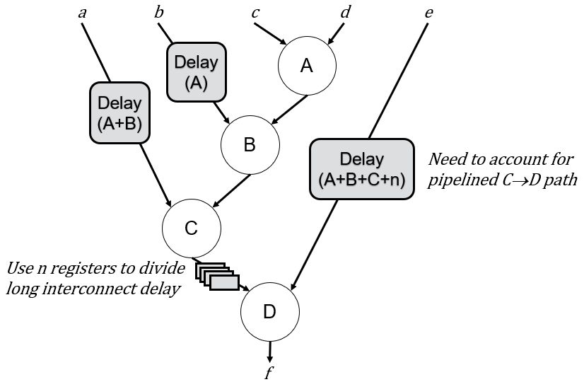
Ultimately, pipelining interconnect ultimately becomes the same problem as balancing pipeline delays. Even when it doesn’t affect other delays, adding registers to one wire will start the whac-a-mole game by changing the placement of the design so that two other modules are now farther apart, and so on. Again, this annoyance is begging to be automated.
Similarly, another common situation in timing optimization is changing the latency of an operation in a datapath that has a corresponding finite-state machine (sometimes called an FSM+D). For example, consider the following abstract FSM+D:
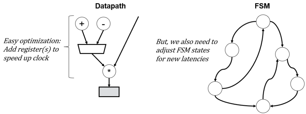
Let’s pretend we’ve created this design, simulated it thoroughly, and then synthesized it only to find out that we can’t run it at a specific clock frequency due to a long combinational path from the add/sub through a mux and multiplier. The immediately obvious optimization is to add registers along that path, which solves the timing problem, but now our design no longer works because the FSM timing was based on the timing of the original datapath.
If we’re lucky, the FSM is simple and can be easily adjusted manually. However, for complex FSMs, it might be much trickier. For example, maybe you are optimizing someone else’s code without any documentation (a reasonably common situation in industry), in which case it is very difficult to adjust the FSM. Again, this optimization is begging to be automated.
How can we enable more automation in FPGA tools?
Did you notice that each of the optimizations in the previous section all did the same thing? They all just added registers. It is a running joke among FPGA engineers that all we do is decide where to put registers. While obviously an exaggeration, there is some truth to it. The vast majority of my time optimizing is spent deciding on where to add or remove registers, and how to adjust the rest of the design accordingly.
Fortunately, this common practice also means that we can potentially solve a massive number of Category 3 problems with a surprisingly simple (conceptually, at least) solution: we need FPGA tools with the flexibility of current RTL synthesis tools, but with the ability to change the timing of the design by adding and removing registers.
Ignoring the details for now of how to enable this functionality in existing tools, let’s first consider the implications of such a tool. First of all, manual timing optimizations would solely focus on minimizing logic delays, which in my experience is considerably easier than optimizing interconnect delays. Even some logic delay bottlenecks could be optimized via automatic pipelining.
In the envisioned tool, a designer would optimize logic delays, set latency and/or clock constraints, specify an optimization goal, and then the tool would explore millions of possibilities that no designer could ever manually explore. Such exploration could be done at all steps of the compilation process. Synthesis could make initial guesses at how many registers might be needed, which is further adjusted during placement based on distances between cells, and fine-tuned during routing to handle congestion. If provided with an understanding of the timing of each net, synthesis could automatically add multi-cycle paths. Dealing with the annoying situation of spacing distant modules with an appropriate number of registers would likely never need to be done manually.
Most importantly, the real significance of this functionality is that it would enable a massive amount of new design-space exploration. The true challenge of FPGA design (and hardware design in general) is finding a solution within a massive solution space that meets all constraints and the provides an attractive result for the optimization goal. Manual exploration is greatly limited by the lengthy compile times, so FPGA designers are in desperate need of help from tools to automate as much of this exploration as possible.
If you aren’t familiar with design-space exploration, I would suggest you first read my article on “Design the Circuit, then Write the Code.” What does it mean to “design a circuit?” For experienced engineers, it means exploring numerous architectural and algorithmic options to determine Pareto-optimal tradeoffs that are attractive for a specific use case. For example, if we are trying to maximize throughput given an area constraint, we probably want to explore options that help maximize clock frequency. Alternatively, if you want to minimize latency given a throughput and area constraint, you are going to have to explore a large number of registering strategies that provide tradeoffs between latency and throughput. Evaluating these different implementation options to find an attractive solution is the basis of design-space exploration. Once you’ve explored a number of solutions and settled on a particular implementation option, you have now designed the circuit and are ready to write code.
As someone who has spent their career on FPGA designs, this design-space exploration is by far the largest percentage of my time, even compared to debugging. If you aren’t spending a lot of time on exploration, you likely have a significant amount of untapped optimization potential.
In my reimagining of FPGA compilation, tools would handle the vast majority of this exploration without any effort from the designer. This exploration includes the previously mentioned timing optimization and pipelining challenges, but extends to almost all aspects of circuit design. You would still need to make some design decisions (e.g., which algorithm to use), but the majority of register-based optimizations would be handled automatically, providing both a massive productivity boost in addition to improving results compared to existing designs.
Why can’t existing tools perform thorough exploration?
RTL synthesis tools actually already perform a huge amount of exploration during synthesis, placement, routing, and physical optimization. However, the effectiveness of that exploration is heavily restricted, not by any fundamental technical limitation, but by restrictions imposed by RTL code.
While RTL code has the important advantage of allowing designers to specify the exact structure and cycle-by-cycle timing of a design, that advantage comes with a significant restriction: the tools are not allowed to change that timing. If there is an optimization that could be applied by adding or removing a cycle, RTL synthesis will not consider it. Although synthesis can adjust the positions of registers within a design (i.e., retiming), the total number of cycles along each path must remain the same.
Because the vast majority of the exploration we need to discover attractive architectural options requires changes to number of cycles, there is no realistic way to incrementally change RTL synthesis. We need to rebuild synthesis from the ground up.
How can we design tools that can change timing?
I originally intended this article to focus on the technical challenges of enabling timing changes during FPGA compilation. However, I quickly realized that the explanation requires a lengthy technical paper by itself, so I’ll hold off on the low-level details and instead provide a high-level overview.
Interestingly, there is already an existing compilation technology with the capability of changing timing: high-level synthesis. High-level synthesis certainly has its place and can compete with custom RTL code in some situations, but it is not mature enough to replace all, or even most, RTL design in my experience.
The primary limitation of HLS is that it removes all custom structure and timing from the circuit. This limitation is intended, since one goal of HLS is to give non-experts, who lack the understanding to choose different structures and timing, the ability to create hardware. However, when RTL code beats HLS, it does so because of the flexibility to create any circuit.
My envisioned solution isn’t to replace RTL or HLS. Instead, I want to combine them into a single specification with a corresponding compilation tool flow that provides the advantages described earlier. When I left academia, I was working on a language that allowed a designer to supplement traditional RTL with higher-level information. For situations benefiting from RTL descriptions, the code would largely resemble existing RTL languages. If a designer didn’t care about structure or timing at all, it would resemble high-level code. However, the novelty is the ability to mix specification styles to achieve the best of both worlds. For example, even for designs specified mostly in RTL, designers would specify regions with flexible timings, such as buses, which would help automate timing closure of interconnect delays during placement and routing. For pipelines with creative structures that are difficult to achieve in HLS, a designer could specify the structure of the pipeline, while specifying that the timing is flexible, with the constraint that all outputs must be aligned. For basic pipelines, designers could use high-level loops like existing HLS.
Another advantage of mixing these design styles with one specification is the automatic integration of functionality from different levels of abstraction. You can use existing HLS to generate pieces of a large design, but you often have to stitch it together with the other parts. If you have a complicated interconnect or network-on-chip, this can be challenging. With my envisioned approach, the integration of different modules would be automatically explored during compilation.
Finally, this new language can enable the envisioned timing-flexible compilation by providing a representation of the program that specifies how to preserve correct behavior during changes to timing. While there are many choices for the specific representation, HLS already does something similar with control/dataflow graphs (CDFGs), which don’t specify any timing, but do specify control and data dependencies. If the compiler adds registers to a set of resources as a timing optimization, the dependencies in the graph provide enough information to know what other components and/or wires need to be delayed accordingly.
With knowledge of how to preserve correct behavior throughout the entire compilation process of synthesis, placement, and routing, this envisioned compiler can solve many Category 3 problems, including the common challenges of delay alignment and timing optimizations.
Conclusions and Future Work
While there are still research challenges to solve, and a massive amount of engineering to prototype this envisioned language and compiler, I believe it has the potential to transform how FPGA applications are developed.
When I left academia, my lab was close to having a working prototype of a placer and router that could add or remove registers to achieve timing closure, while preserving semantic correctness. I was also working on combining functionality from existing HLS and RTL tools to provide mixed-abstraction design entry. The timeline for finishing those projects is now indefinite, so if anyone wants to collaborate, let me know and hopefully we can find a way to make this envisioned solution possible.
Acknowledgements
I’d like to acknowledge all the former PhD, MS, and undergrad students that contributed to this project. I apologize if I forget a few people, but this list includes Benjamin Wheeler, Bryan Kristofferson, Cole Johnson, Keeth Smith, and Alex Rodriguez. Special thanks to Austin Baylis and Madison Emas, who led different parts of the project. I have never been more excited about a project, so it’s unfortunate we didn’t get to publish this, but I wanted to make sure everyone involved received recognition for their hard work.
References
- D. Wilson, G. Stitt, and J. Coole, “A recurrently generated overlay architecture for rapid fpga application development,” in Proceedings of the 9th International Symposium on Highly-Efficient Accelerators and Reconfigurable Technologies, HEART 2018, pp. 4:1–4:6, ACM, June 2018.
- J. Coole and G. Stitt, “Adjustable-cost overlays for runtime compilation,” in Field-Programmable Custom Computing Machines (FCCM), 2015 IEEE 23rd Annual International Symposium on, pp. 21–24, May 2015.
- J. Coole and G. Stitt, “Fast, flexible high-level synthesis from OpenCL using reconfiguration contexts,” Micro, IEEE, vol. 34, pp. 42–53, Jan 2014.
- A. Landy and G. Stitt, “A low-overhead interconnect architecture for virtual reconfigurable fabrics,” in CASES’12: Proceedings of the 2012 international conference on Compilers, architectures and synthesis for embedded systems, CASES ’12, (New York, NY, USA), pp. 111–120, ACM, October 2012.
- J. Coole and G. Stitt, “Intermediate fabrics: Virtual architectures for circuit portability and fast placement and routing,” in CODES/ISSS ’10: Proceedings of the IEEE/ACM/IFIP international conference on Hardware/Software codesign and system synthesis, pp. 13–22, October 2010.