
If you’ve studied digital design, you have likely used a field-programmable gate array (FPGA) to implement custom circuits. This widespread use of FPGAs stems from their flexible and reconfigurable architecture, which can support potentially any register-transfer level (RTL) design.
However, unless you have deployed a highly constrained FPGA application, you might not have considered how to optimize your RTL code for a specific FPGA. While application-specific integrated circuits (ASICs) and FPGAs can often use similar RTL code, optimizing a design for a particular FPGA requires careful consideration.
In this article, we’ll examine a simple example using commonly employed RTL code and demonstrate how to optimize it specifically for an FPGA to improve performance, reduce resources, and provide different trade-offs.
Comparing ASICs and FPGAs
Before looking at FPGA-specific optimizations, it is important to understand the differences between FPGAs and ASICs to recognize optimization opportunities.
Both ASICs and FPGAs provide a set of computational primitives called cells. When you synthesize your design, the synthesis tool performs technology mapping to map your design onto the available cells. For ASICs, you must specify a cell library, which is usually provided by a foundry for a specific process technology. ASIC cell libraries generally consist of hundreds of fine-grained cell primitives but increasingly contain coarse-grained cells like multipliers, adders, etc.
By contrast, FPGA synthesis tools come with a predefined cell library that is chosen when you select a specific FPGA. Unlike ASICs, FPGA cell libraries usually feature a smaller number of coarse-grained cell types, including lookup tables (LUTs), DSP blocks, configurable logic blocks (CLBs), and memory blocks, as well as fine-grained cells like flip-flops.
Another key distinction is the fixed physical placement of the cells in an FPGA. When designing an ASIC, you can utilize any amount and type of cell, and the placer can position them based on your application’s needs. By contrast, FPGA placement maps a design’s cell instances onto predefined physical cells.
Routing also differs significantly between FPGAs and ASICs. FPGA routing resources are physically placed during device fabrication but come with reconfigurable capabilities. In ASICs, routing resources are allocated after placement, offering greater flexibility.
Additionally, ASICs allow for the “sizing” of cells and transistors to provide different area and delay trade-offs. Interestingly, optimizing for area in the traditional sense is not applicable for FPGAs due to their fixed resource allocation. Instead, FPGA optimization focuses on resource utilization, often informally referred to as “area,” reflecting their original use for ASIC prototyping.
FPGA Optimization Strategies
Now that we understand the basic differences between ASICs and FPGAs, how can we use this information to modify our RTL code to more effectively utilize FPGAs?
There are several fundamental strategies to consider:
- Strategy 1: Leverage unique FPGA cells types.
- Strategy 2: Utilize unused resources.
- Strategy 3: Exploit dynamic reconfiguration.
To implement Strategy 1, evaluate whether your design can better capitalize on the unique features of LUTs, small RAMs, DSP blocks, and the low-level functionalities provided by different CLBs (such as muxes, adders, and carry chains). Compared to ASIC cell libraries, these FPGA cells are often more coarse grained. While these cells can be used to implement arbitrary RTL code, a design can often be made more efficient by explicitly specializing the design to directly target specific cell types. While general recommendations for applying this strategy can be elusive and require some creativity, the example provided in this article should offer useful insights.
Strategy 2 involves a shift in perspective from ASIC design. In ASICs, you typically avoid adding resources that don’t contribute directly to functionality due to concerns about increased area and/or power. However, in FPGAs, there are millions of available resources that might otherwise go unused. For example, while an ASIC would include embedded memory only when necessary, an FPGA offers thousands of small memories that can be utilized in creative ways. Basically, in an FPGA, the resources are there whether or not you need them, so you might as well try to find a use for them unless you have tight power constraints.
Strategy 3 highlights one of the most distinctive features of FPGAs: the ability to dynamically reconfigure hardware. This capability enables a wide range of potential applications and even offers unique advantages over ASICs. While a comprehensive discussion of dynamic reconfiguration is beyond the scope of this article, we hope to explore it in more detail in the future.
In the following example, we will apply Strategies 1 and 2 to optimize a typical RTL design to target an UltraScale+ FPGA.
Example: counting ones
The module we will explore has a single input data, whose width is specified by a parameter WIDTH. The module’s output count specifies the number of input bits that are asserted.
Let’s begin with one of the simplest and most common ways to implement this functionality:
module count_ones_simple1 #(
    parameter int WIDTH = 16
) (
    input  logic [          WIDTH-1:0] data,
    output logic [$clog2(WIDTH+1)-1:0] count
);
    always_comb begin
        count = '0;
        for (int i = 0; i < WIDTH; i++) begin
            count += data[i];
        end
    end
endmodule
In this implementation, the module iterates over each bit of the data input, accumulating a count of asserted bits to generate the output. Note that the count output is $clog2(WIDTH+1) bits wide, which can be confusing. As you may know, $clog2(x) determines the number of bits needed to represent x different values. Since count ranges from 0 to WIDTH, it encompasses WIDTH+1 possible values. Using $clog2(WIDTH) instead of $clog2(WIDTH+1) is a common error, often overlooked in simulation unless the testbench explicitly checks relevant cases.
Next, let’s examine the elaborated schematic in Vivado to verify that the circuit matches our expectations:
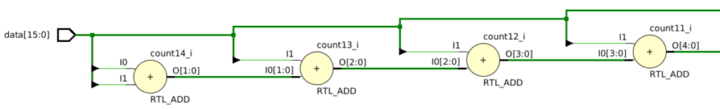
As expected, the schematic shows that Vivado chains together adders. A potential limitation of this implementation is that delay increases linearly with width, similar to a ripple-carry adder. We will soon evaluate the module to determine whether synthesis can optimize it and mitigate this linear delay increase.
Before we perform that evaluation, let’s consider another implementation where we similarly iterate across all input bits and add one to the count if the bit is asserted:
module count_ones_simple2 #(
    parameter int WIDTH = 16
) (
    input  logic [          WIDTH-1:0] data,
    output logic [$clog2(WIDTH+1)-1:0] count
);
    always_comb begin
        count = '0;
        for (int i = 0; i < WIDTH; i++) begin
            if (data[i]) count += 1'b1;
        end
    end
endmodule
Next, let’s take a look at a snippet of the elaborated schematic:
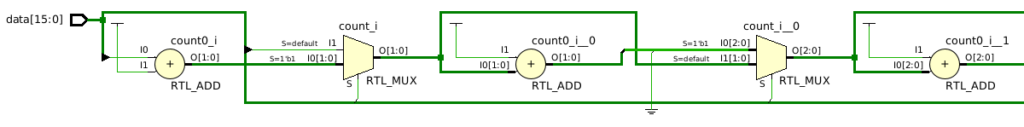
Interestingly, Vivado uses a significantly different circuit for this implementation, underscoring the importance of reviewing the schematic to ensure it aligns with expectations. In this case, the if statement is translated into a multiplexer (mux) that selects between the previous count and the updated count based on data[i].
At first glance, the schematic might suggest that this module is less efficient, as it uses muxes in addition to adders. While this assumption seems reasonable, FPGA synthesis tools can produce unexpected results. Therefore, we’ll need to confirm its inefficiency before dismissing it.
The table below shows the LUT usage for each module across different widths:
| WIDTH: | 2 | 4 | 8 | 16 | 32 | 64 | 128 |
|---|---|---|---|---|---|---|---|
| simple1 | 1 | 2 | 8 | 25 | 53 | 113 | 230 |
| simple2 | 1 | 2 | 7 | 20 | 55 | 102 | 228 |
As expected, both designs show a roughly linear increase in LUT counts with increasing widths. Surprisingly, the count_ones_simple2 module generally used fewer LUTs than the count_ones_simple1 module. This result is unexpected, give that count_ones_simple2 used muxes and adders, whereas count_ones_simple1 only used adders. We’ll explore the reasons for this unexpected result in a future article. However, this situation highlights an important point: it’s not uncommon for synthesis tools like Vivado to produce surprising results. These tools can counterintuitively optimize additional components in ways that lead to a smaller circuit after technology mapping.
Does this mean that count_ones_simple2 is the better implementation? To answer this question, we also need to consider the delay of the longest path across different widths:
| WIDTH: | 2 | 4 | 8 | 16 | 32 | 64 | 128 |
|---|---|---|---|---|---|---|---|
| simple1 | 0.404 | 0.512 | 0.782 | 0.906 | 1.171 | 1.477 | 1.946 |
| simple2 | 0.404 | 0.512 | 0.799 | 0.931 | 1.348 | 1.676 | 2.626 |
Although count_ones_simple2 generally required the fewest LUTs, it also exhibited increasingly worse delays as the width increased. This illustrates a phenomenon known as Pareto optimality. Neither implementation is strictly better than the other; one is smaller but slower, while the other is larger but faster. An implementation is considered “Pareto optimal” if there is no other known implementation that is better in all relevant metrics.
FPGA Optimization: Lookup Tables
With our baseline implementations established, we can now explore how to apply the strategies discussed earlier. For Strategy 1, let’s consider how we can leverage the unique characteristics of an FPGA to potentially reduce resources and/or delay. One common optimization technique is to implement combinational logic functions using lookup tables. In fact, Vivado already did this when synthesizing the two simple modules, mapping the adders and multiplexers onto the small physical LUTs provided by the FPGA. However, our goal is to take a different approach: we aim to modify our implementation to directly utilize these LUTs in a way that Vivado has not fully exploited.
Before we proceed, it’s important to distinguish between logical lookup tables and physical lookup tables in an FPGA. Logical lookup tables are a general strategy for replacing computations with a table that contains all pre-computed outputs, independent of the specific resources used. Physical lookup tables, on the other hand, are FPGA resources designed to implement logical lookup tables of specific sizes.
To avoid confusion, we will use “logical lookup table” to refer to the general concept and “physical lookup table” for the FPGA resource. We’ll also reserve the acronym “LUT” for the physical resource, which is a common convention.
First, let’s explore one extreme possibility. For combinational logic, an n-input function can always be implemented using an n-input lookup table. In theory, we could replace the entire design with a single WIDTH-input lookup table for each output. However, an n-input lookup table requires 2n rows, meaning that as n increases, the table size grows exponentially. This rapid scaling makes this approach impractical for large widths. Nevertheless, for smaller widths, it is feasible to replace a sequence of adders with a single lookup table.
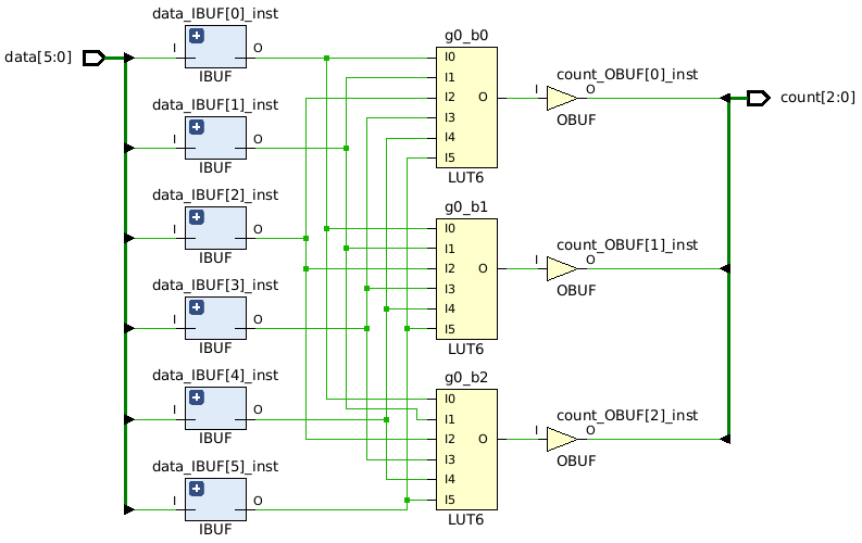
One natural question is: for what widths is the lookup table strategy efficient? To answer this, we need to examine the details of our target FPGA. We will focus on the UltraScale+ family, which features LUTs with 6 inputs and 1 output. This means that as long as WIDTH ≤ 6, we can implement the entire functionality using a single LUT for each output bit. For example, for a WIDTH of 6, the count output requires 3 bits, so we would only need three LUTs in total. We can confirm this by examining the synthesized schematic:
Let’s look at the code we used to synthesize this schematic:
module count_ones_lut #(
    parameter int WIDTH = 6
) (
    input  logic [          WIDTH-1:0] data,
    output logic [$clog2(WIDTH+1)-1:0] count
);
    localparam int COUNT_WIDTH = $clog2(WIDTH + 1);
    typedef logic [COUNT_WIDTH-1:0] rom_array[2**WIDTH];

    function rom_array init_lookup();
        automatic rom_array counts = '{default: '0};
        for (int unsigned i = 0; i < 2 ** WIDTH; i++) begin
            counts[i] = (i & 1) + counts[i/2];
        end
        return counts;
    endfunction

    logic [COUNT_WIDTH-1:0] rom[2**WIDTH] = init_lookup();
    assign count = rom[data];
endmodule
This code essentially creates a ROM, which the synthesis tool maps into LUTs. The ROM is inferred from lines 18-19 of the code. However, we need a method to specify the ROM contents. Typically, designers use a memory initialization file to define the contents separately from the code. Unfortunately, in this case, a separate file isn’t practical, as it would require a different file for each possible width.
Instead, the code computes the ROM contents during elaboration (one of the initial steps of synthesis). Specifically, the ROM is initialized by the init_lookup() function on line 18. This function uses a loop to iterate over all 2WIDTH rows of the lookup table, with each iteration applying dynamic programming to compute the correct count output.
If you’re not familiar with SystemVerilog, some of the syntax might be confusing. The init_lookup() function needs to return an array that matches the size of the rom signal on line 18. Since there is no direct way to achieve this, we use the typedef construct to define the desired type, which can then be returned from the function.
We now have an ultra-efficient implementation for small widths. However, for widths greater than 6, the resource requirements increase exponentially. Therefore, this approach is not suitable as a general solution.
Fortunately, there are other options. Let’s try a hybrid solution where we decompose the input into 6-bit “slices,” use lookup tables to compute the counts for each slice, and then sum these counts. This approach combines elements of the original count_ones_simple1 module—where we added all the bits—but reduces the number of adders (and their associated delays) by using lookup tables to precompute the counts before performing the addition.
An initial attempt at this approach might look something like this:
module count_ones_hybrid1 #(
    parameter int WIDTH = 18
) (
    input  logic [          WIDTH-1:0] data,
    output logic [$clog2(WIDTH+1)-1:0] count
);
    localparam int LOOKUP_WIDTH = 6;
    localparam int COUNT_WIDTH = $clog2(WIDTH + 1);
    localparam int NUM_SLICES = $ceil(real'(WIDTH) / LOOKUP_WIDTH);

    logic [COUNT_WIDTH-1:0] slice_count[NUM_SLICES];

    for (genvar i = 0; i < NUM_SLICES; i++) begin : l_slices
        count_ones_lut #(
            .WIDTH(LOOKUP_WIDTH)
        ) slices (
            .data (data[LOOKUP_WIDTH*(i+1)-1-:LOOKUP_WIDTH]),
            .count(slice_count[i])
        );
    end

    always_comb begin
        count = '0;
        for (int i = 0; i < NUM_SLICES; i++) begin
            count += slice_count[i];
        end
    end
endmodule
Lines 22-27 are adapted from the original count_ones_simple1 module but now add the counts of the slices instead of individual bits. The remainder of the code is responsible for generating these slices. The number of slices is determined by WIDTH / LOOKUP_WIDTH, where LOOKUP_WIDTH is 6 to match the UltraScale+ LUTs. Since this division can result in a remainder, we need to round up to the next integer using $ceil.
After determining the number of slices, lines 13-20 instantiate our earlier count_ones_lut module to look up the count for each slice.
One significant limitation of this module is that it requires WIDTH to be a multiple of LOOKUP_WIDTH, which is quite restrictive. While we can extend the module to support any width, we’ll explore other possibilities first.
Earlier, I clarified the difference between logical and physical lookup tables. Essentially, a logical lookup table can be implemented using various types of memory. FPGAs have millions of small LUT memories, but they also feature larger embedded memories, such as block RAM and UltraRAM for UltraScale+.
Block RAMs can usually be configured to support different depths and widths. For UltraScale+, in their deepest configuration, they provide 32k rows, with each row being a single bit. With 32k rows, we could implement a 15-input logic function (since 215=32k). A width of 15 would require 4 bits for the count output, so we could potentially use 4 block RAMs to implement our module for widths up to 15.
Alternatively, the block RAMs can also be configured with 16k rows, where each row is 2 bits. This would support a 14-input logic function (since 214=16k), but we would still need four block RAMs for a width of 14, one for each output bit.
An interesting configuration for our purposes is 8k rows with 4 bits per row. This setup allows us to implement a width of 13 in a single block RAM, making it a strong candidate for our hybrid approach.
Before we modify the hybrid approach, let’s update our lookup approach to use block RAM instead of LUTs:
module count_ones_bram #(
    parameter int WIDTH = 13
) (
    input  logic                       clk,
    input  logic [          WIDTH-1:0] data,
    output logic [$clog2(WIDTH+1)-1:0] count
);
    localparam int COUNT_WIDTH = $clog2(WIDTH + 1);
    typedef logic [COUNT_WIDTH-1:0] rom_array[2**WIDTH];

    function rom_array init_lookup();
        automatic rom_array counts = '{default: '0};
        for (int unsigned i = 0; i < 2 ** WIDTH; i++) begin
            counts[i] = (i & 1) + counts[i/2];
        end
        return counts;
    endfunction

    (* rom_style="block" *) logic [COUNT_WIDTH-1:0] rom[2**WIDTH] = init_lookup();
    always_ff @(posedge clk) begin
        count <= rom[data];
    end
endmodule
This code is almost identical to the earlier count_ones_lut module, with a few key differences on lines 19-22. Line 19 uses the rom_style attribute to explicitly instruct Vivado to use block RAM. While this attribute may not always be necessary, it ensures Vivado doesn’t default to another type of memory resource. Lines 20-22 read from the ROM with a 1-cycle delay, which is required because block RAMs have a 1-cycle read latency. Attempting to output the count in the same cycle as the read operation could prevent Vivado from inferring a block RAM correctly. Generally, synthesis tools provide coding guidelines to help infer different types of RAM resources.
Now that we have two methods for leveraging logical lookup tables—using LUTs and block RAM—we can combine them into a single module that selects the appropriate resource based on the requested width.
module count_ones_rom #(
    parameter int WIDTH = 16
) (
    input  logic                       clk,
    input  logic [          WIDTH-1:0] data,
    output logic [$clog2(WIDTH+1)-1:0] count
);
    localparam int COUNT_WIDTH = $clog2(WIDTH + 1);
    typedef logic [COUNT_WIDTH-1:0] rom_array[2**WIDTH];

    function rom_array init_lookup();
        automatic rom_array counts = '{default: '0};
        for (int unsigned i = 0; i < 2 ** WIDTH; i++) begin
            counts[i] = (i & 1) + counts[i/2];
        end
        return counts;
    endfunction

    if (WIDTH <= 6) begin : l_luts
        logic [COUNT_WIDTH-1:0] rom[2**WIDTH] = init_lookup();
        assign count = rom[data];
    end else begin : l_bram
        (* rom_style="block" *) logic [COUNT_WIDTH-1:0] rom[2**WIDTH] = init_lookup();
        always_ff @(posedge clk) begin
            count <= rom[data];
        end
    end
endmodule
This new count_ones_rom module simply combines the two previous implementations using an if-generate construct. For widths less than or equal to 6, it instantiates the LUT-based implementation. For all other widths, it uses the block RAM implementation.
Finally, we can create a new hybrid approach that has an additional parameter USE_BRAM. Depending on the value of this parameter, the module will decompose itself into 6-bit slices (for LUTs), or 13-bit slices (for block RAM). Here is the code:
module count_ones_hybrid2 #(
    parameter int WIDTH = 64,
    parameter bit USE_BRAM = 1'b1
) (
    input  logic                       clk,
    input  logic [          WIDTH-1:0] data,
    output logic [$clog2(WIDTH+1)-1:0] count
);
    localparam int LOOKUP_WIDTH = USE_BRAM ? 13 : 6;
    localparam int SLICE_COUNT_WIDTH = $clog2(LOOKUP_WIDTH + 1);
    localparam int NUM_SLICES = $ceil(real'(WIDTH) / LOOKUP_WIDTH);

    logic [SLICE_COUNT_WIDTH-1:0] slice_count[NUM_SLICES];
    logic [NUM_SLICES*LOOKUP_WIDTH-1:0] data_expanded;

    always_comb begin
        data_expanded = '0;
        data_expanded[WIDTH-1:0] = data;
    end

    generate
        for (genvar i = 0; i < NUM_SLICES; i++) begin : l_slices
            count_ones_rom #(
                .WIDTH(LOOKUP_WIDTH)
            ) slices (
                .clk  (clk),
                .data (data_expanded[LOOKUP_WIDTH*(i+1)-1-:LOOKUP_WIDTH]),
                .count(slice_count[i])
            );
        end
    endgenerate

    always_comb begin
        count = '0;
        for (int i = 0; i < NUM_SLICES; i++) begin
            count += slice_count[i];
        end
    end
endmodule
In addition to enabling the use of block RAM or LUTs, this code addresses the restriction of requiring WIDTH to be a specific multiple of the slice width. Various approaches could have been used, but a simple solution was to introduce an internal data_expanded signal. This signal expands the data input to the next higher multiple of the lookup/slice width. Any unused bits in data_expanded are initialized to 0, allowing synthesis tools to optimize them away.
Results
Let’s now compare the LUT usage and delay of the two original baseline implementations with the final count_ones_hybrid2 module, including both LUTs and block RAM (BRAM). The results for LUT usage are shown below:
| WIDTH: | 2 | 4 | 8 | 16 | 32 | 64 | 128 |
|---|---|---|---|---|---|---|---|
| simple1 | 1 | 2 | 8 | 25 | 53 | 113 | 230 |
| simple2 | 1 | 2 | 7 | 20 | 55 | 102 | 228 |
| hybrid2 (LUTs) | 1 | 2 | 6 | 17 | 38 | 86 | 169 |
| hybrid2 (BRAM) | 0 | 0 | 0 | 5 | 14 | 25 | 63 |
As expected, the count_ones_hybrid2 LUT implementation used considerably fewer LUTs compared to both original baseline implementations. The block RAM version of count_ones_hybrid2 used even fewer LUTs, which aligns with the goal of that implementation: to replace LUTs with block RAM. Although block RAM usage isn’t shown in the table, it ranged from 1 block RAM for widths from 2 to 16 bits, 2 block RAMs for 32 bits, 3 block RAMs for 64 bits, and 5 block RAMs for 128 bits.
Interestingly, while a single block RAM was anticipated for widths up to 13 bits, the 16-bit width still required only 1 block RAM, despite the code explicitly instantiating 2. It seems Vivado recognized that the second slice had very low utilization (only 3 inputs) and converted the block RAM into LUTs. Although Vivado is not supposed to do this when using the “block” ROM_STYLE attribute, it demonstrates a useful optimization for different trade-offs. Similarly, for 32 bits, which should have required 3 block RAMs, Vivado again used LUTs for the final slice. This trend continued for larger widths, with increasing amounts of LUTs being used. A detailed investigation into what exactly Vivado did is beyond the scope of this article, but we may revisit this in a future post in my RTL Code is Weird series.
Next, let’s look at the delay results:
| WIDTH: | 2 | 4 | 8 | 16 | 32 | 64 | 128 |
|---|---|---|---|---|---|---|---|
| simple1 | 0.404 | 0.512 | 0.782 | 0.906 | 1.171 | 1.477 | 1.946 |
| simple2 | 0.404 | 0.512 | 0.799 | 0.931 | 1.348 | 1.676 | 2.626 |
| hybrid2 (LUTs) | 0.411 | 0.491 | 0.727 | 0.822 | 1.153 | 1.496 | 1.863 |
| hybrid2 (BRAM) | 0.772 | 0.772 | 0.772 | 1.689 | 1.779 | 2.176 | 2.39 |
With a few minor exceptions, the hybrid LUT-based architecture provided the best delay overall. While there is technically no single “best” solution across all widths, the hybrid LUT architecture is perhaps the closest we have to an optimal design. It achieves the smallest design in terms of LUTs (excluding block RAM) and has either the best or comparable delay.
The hybrid block RAM architecture generally had a delay that was worse than all other implementations. In addition, that delay was somewhat optimistic, as it requires an additional cycle compared to the other methods. If we had added a register to the other implementations to match the latency of the block RAM approach, their delays could potentially be halved. Despite this, the hybrid block RAM architecture remains a Pareto-optimal solution because it uses the fewest LUTs. If minimizing LUT usage is the primary goal and the clock constraints are achievable, then the hybrid block RAM architecture could be the most attractive option for that use case.
The hybrid LUT architecture almost eliminates the Pareto optimality of the simple2 architecture, as it is better in terms of both LUTs and delay in all situations except for the slightly worse delay for a width of 2.
Further Exploration
The exploration in this article is far from exhaustive. In reality, there are numerous other options we could investigate. For example, we reasoned that a block RAM address width of 13 bits would provide an efficient lookup table, but we didn’t actually explore any other widths to confirm this. As we have seen, synthesis tools can yield surprising results depending on the design and FPGA, so it’s entirely possible that our reasoning was based on inaccurate assumptions.
In addition, we only considered one type of slice in our hybrid architecture. It could be beneficial to mix block RAM and LUTs to handle widths that aren’t multiples of either address width. For instance, to support a width of 19, we could use one slice with a LUT and another with a block RAM. For larger widths, there are many possible combinations to explore.
We also only considered block RAM, but UltraScale+ FPGAs also include UltraRAM. Although UltraRAM has a fixed configuration of 4k rows with 72 bits per row, it could potentially be wrapped with additional logic to create custom configurations. This approach would introduce even more resource combinations to explore for a given width.
We also didn’t explore pipelining, which could significantly reduce the longest delays for each design at the expense of increased latency. In pipelined designs, the hybrid approach might offer substantial advantages, as it minimizes the number of adders and thus could lead to more pronounced latency improvements.
Although it’s not immediately clear how DSP blocks could be beneficial in this context, there may be ways to leverage them to achieve different trade-offs.
Finally, I had expected the delays of the count_ones_simple1 module to be sub-linear. Typically, a synthesis tool will convert a sequence of adders into an adder tree, which we’ve explored in previous articles. Synthesis usually achieves this goal by applying an optimization called tree-height reduction, which should make the delay increase logarithmically with width rather than linearly. I didn’t investigate which optimizations Vivado applied, but if it wasn’t performing tree-height reduction, I would manually implement it by instantiating a combinational adder tree. Note, however, that despite the logarithmic logic-delay advantage of an adder tree, it doesn’t always guarantee reduced overall delay. FPGA architectures are highly optimized for carry chains found in adder sequences. In adder trees, synthesis tools might not leverage these carry chains as effectively, which can lead to interconnect delays that might outweigh the logarithmic logic delay at certain widths. This could explain why Vivado didn’t exploit it. Perhaps we’ll explore this in a future article.
Additional Considerations
Synthesis tools and simulators often have limited support for language standards, which means that some examples in this article may not work across all platforms. For instance, I’ve encountered tools that did not support the $ceil function, requiring me to create a custom implementation. A common issue you might face with the examples here is related to the init_lookup() function used for initializing lookup tables. This function depends on synthesis tools being able to handle extensive code during elaboration. Most tools impose a limit, generating an error if elaboration exceeds a certain threshold. For example, in Quartus Prime Pro, an error message indicates that loops can only iterate up to 5000 times during elaboration. Consequently, this constraint means that lookup tables must have 4k row (12-bit addresses) or fewer to avoid errors.
Conclusions
In this article, we explored several strategies for optimizing hardware specifically for FPGAs. We demonstrated that even simple examples can leverage FPGA-specific resources to achieve non-obvious optimizations and trade-offs.
You might wonder which implementation I would typically use, which is a great question. Most methodologies discourage “pre-optimization,” as it often leads to significant time wasted on premature adjustments that may not be necessary. For the example discussed in this article, I would start with the count_ones_simple1 module because it’s the most straightforward. I would then explore other options only if count_ones_simple1 revealed resource or timing bottlenecks.
However, if I anticipate a significant bottleneck that could prevent meeting optimization goals or constraints, I would immediately engage in design-space exploration. At the start of any new application, I usually conduct a high-level design-space exploration to understand possible trade-offs and identify solutions that can meet the constraints. I would then expand my exploration to lower-level modules, like the example in this article, if they become bottlenecks within the overall design.
Finally, and most importantly, I hope you’re starting to see a trend in many of my articles: even trivially simple modules can have massive amounts of different implementations. Developing the ability to identify and explore these solutions—known as design-space exploration—is what truly sets experts apart from other designers.