
RAMs are a fundamental part of most digital designs, yet there’s still no widely adopted RTL template for inferring RAMs that works reliably across all FPGAs. As a result, many designers resort to manually instantiating RAM primitives or using vendor-specific IP cores. While this approach gets the job done, it’s often tedious and undermines portability—one of the key reasons RTL design is notoriously unproductive. A more efficient and portable alternative is to infer RAMs directly from RTL, but this requires carefully crafted templates to ensure synthesis tools map the logic to the intended memory resources.
The goal of this article is to provide and explain a set of customizable RAM inference templates that work across most FPGAs. While it’s nearly impossible to create a one-size-fits-all template that captures every low-level RAM feature across all devices, the templates here cover the most common functionality needed in typical designs. If you need a specialized RAM feature for a particular FPGA, chances are it’s easy to extend or adapt the templates accordingly.
These templates have been tested in both Vivado and Quartus Prime Pro. Since RAM architectures vary across FPGA families, I haven’t tested them on every device—but I’ve used variations of these templates for over a decade and haven’t yet encountered a case I couldn’t support with minor adjustments.
All SystemVerilog code is available on GitHub as part of my SystemVerilog tutorial. There are also VHDL equivalents on my VHDL tutorial. Interestingly, the VHDL versions require fewer tool-specific workarounds, and work in all versions of Quartus that I have tested. Although I usually aim to write code that works in any synthesis tool, I’ve dropped SystemVerilog support for the non-pro versions of Quartus. The non-pro versions lack support for many SystemVerilog features, which made it difficult to maintain clean and elegant code. While it’s possible to modify the templates to work around those limitations, I chose to prioritize clarity and maintainability over broader tool compatibility.
Background
Before diving into the templates, it’s important to understand the distinction between logical and physical memories, and the different types of each. Physical memories are the actual memory resources available on a specific FPGA, while a logical memory (sometimes called a virtual memory) is the application-specific memory you describe in RTL. Logical memories don’t need to match the functionality of the physical memories exactly, as long as the synthesis tool can implement the intended behavior using some combination of memory blocks and logic. That said, when optimizing logical memories for FPGAs, it’s usually a good idea to understand the underlying memory resources to ensure efficient mapping.
Each FPGA vendor uses slightly different terminology for their physical memory types, but to keep things simple, I’ll group them into two categories: block RAM and distributed RAM.
Distributed RAM typically uses individual LUTs as small memories—after all, that’s essentially what LUTs are. Instead of storing truth tables for combinational logic, we repurpose them to store arbitrary data. Because these LUTs are spread across the FPGA fabric, this type of memory is called distributed RAM.
Distributed RAM has some notable characteristics. Most importantly, it provides asynchronous reads, which makes sense when you consider that LUTs are inherently combinational. It wouldn’t be possible to implement logic functions otherwise. That said, you can get synchronous reads from distributed RAM by adding flip-flops to either the address lines or the output. Distributed RAM also tends to have more limited features compared to block RAM—such as tighter restrictions on depth and width, and often a lack of true dual-port support. It’s also much smaller in total memory capacity.
Different vendors refer to distributed RAM using different terms. In Xilinx/AMD devices, you’ll encounter names like LUTRAM and SLICEM. Xilinx FPGAs generally have two types of slices: SLICEL, where LUTs are used strictly for logic, and SLICEM, where LUTs can be used for both logic and RAM. On the Intel/Altera side, a LAB is analogous to a SLICEL, while an MLAB is similar to a SLICEM, with LUTs that can act as memory.
Block RAM is a more traditional SRAM-based memory and almost always requires synchronous reads. Most modern FPGAs offer a wide range of configuration options for block RAMs, including various depth and width combinations, multiple dual-port modes, registered outputs, and more.
In Xilinx/AMD devices, this type of memory is usually referred to simply as block RAM, though newer devices also include a specialized variant called UltraRAM. UltraRAM is optimized for wide data widths (e.g., 72 bits) and complements standard block RAM for large memory structures. On the Intel/Altera side, block RAMs are generally called embedded memory blocks, with several types available, such as M9K, M20K, and M144K, depending on the device family and memory size.
Most block RAMs follow a port structure similar to the figure below, featuring two independent ports. Each port can typically be configured for either reading or writing, and in some FPGAs, a read may occur implicitly during a write. This architecture is commonly referred to as a true dual-port (TDP) RAM, since both ports operate independently and can access the memory simultaneously.
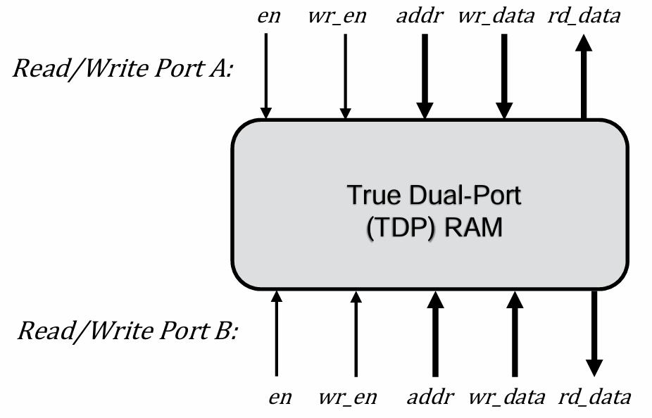
While exact port structures vary across FPGAs, each port always includes an address input (addr), used for both reads and writes, a write data input (wr_data), and a read data output (rd_data). There is also always a write enable (wr_en) signal to control write operations. Some FPGAs include an additional enable signal (en). When this enable is deasserted, the port performs no operation and usually preserves the read data output. When asserted, the port either reads or writes depending on the state of the write enable. For FPGAs without an enable signal, the RAM may perform both a read and a write to the specified address in the same cycle, with the exact behavior varying by device.
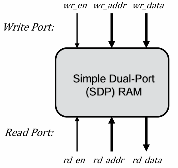
Alternatively, older FPGAs (and most distributed RAM types in newer FPGAs) provide simple dual-port (SDP) RAMs. In these RAMs, there are still two ports, but one is read-only and the other is write-only:
It’s important to note that while you can’t implement a logical TDP memory on top of physical SDP RAM, you can implement a logical SDP memory on top of physical TDP RAM. In fact, this is likely what synthesis tools are doing for you automatically in many designs. From my experience, logical SDP RAMs are much more commonly used than TDP RAMs, although I often use TDP RAMs to optimize designs. In the following sections, I’ll show you how to create inference templates for both SDP and TDP RAMs that can be mapped to different types of physical RAM resources. While single-port RAMs can also be inferred, I won’t cover that explicitly in this article, as I rarely use single-port RAM.
Inferring Simple Dual-Port (SDP) RAMs
We’ll start by exploring templates for logical SDP RAMs, beginning with a basic version and gradually adding functionality until we reach a general-purpose template that can be adapted for most FPGAs. As mentioned earlier, these logical SDP templates can be synthesized onto both physical SDP and TDP memories. We’ll look at examples where the synthesis tool maps the design entirely onto a RAM resource, and others where it introduces additional logic. Both outcomes are acceptable, but if you’re optimizing for a specific FPGA, it’s often a good idea to minimize extra logic—especially if it extends the read data path, which is a common source of timing issues.
Basic SDP Template
If you only need simple memory functionality, the following template should work on any modern FPGA and with nearly any synthesis tool:
module ram_sdp_basic #(
    parameter int DATA_WIDTH = 16,
    parameter int ADDR_WIDTH = 10
) (
    input  logic                  clk,
    input  logic                  rd_en,
    input  logic [ADDR_WIDTH-1:0] rd_addr,
    output logic [DATA_WIDTH-1:0] rd_data,
    input  logic                  wr_en,
    input  logic [ADDR_WIDTH-1:0] wr_addr,
    input  logic [DATA_WIDTH-1:0] wr_data
);
    logic [DATA_WIDTH-1:0] ram[2**ADDR_WIDTH];

    always_ff @(posedge clk) begin
        if (wr_en) ram[wr_addr] <= wr_data;
        if (rd_en) rd_data <= ram[rd_addr];
    end
endmoduleOne of the challenges in creating a portable RAM inference template is that even a basic version like this may include functionality not directly supported by all physical RAM resources. For example, the template includes a read enable (rd_en) that allows the read data output (rd_data) to be preserved when reads are disabled. While most modern FPGAs can synthesize this behavior, not all physical RAM blocks include native support for a read enable. In those cases, the synthesis tool will typically insert additional logic to emulate the desired behavior.
This extra logic is usually fine, but in some designs, I’ve seen it introduce unexpected timing bottlenecks—especially if it ends up on a critical path. If you don’t need a read enable, you can remove it from the template. But there’s often an easier approach: just tie the rd_en signal high when instantiating the RAM. Most synthesis tools will recognize this and optimize the enable logic away, resulting in a clean mapping to the underlying RAM block.
One critically important thing to be aware of with any SDP RAM is the behavior during a simultaneous read and write to the same address—commonly called a “read-during-write” condition. Since the read and write ports operate independently, it’s entirely possible for them to target the same address in a given cycle. In this case, there are typically two outcomes: the read returns either the previous data stored in memory (“read-first”) or the new data being written (“write-first”).
This basic template uses read-first behavior, which I strongly recommend for most designs. While write-first behavior is advantageous in some situations, it often requires extra logic and routing that can reduce the maximum clock frequency by a surprising amount. I’ll cover these kinds of memory tradeoffs in more detail in a separate article.
Write-First SDP Templates
If you need write-first behavior during a read-during-write condition, the following template is one way to achieve it—though it’s not a method I recommend.
module ram_sdp_write_first_inferred #(
    parameter int DATA_WIDTH = 16,
    parameter int ADDR_WIDTH = 10
) (
    input  logic                  clk,
    input  logic                  rd_en,
    input  logic [ADDR_WIDTH-1:0] rd_addr,
    output logic [DATA_WIDTH-1:0] rd_data,
    input  logic                  wr_en,
    input  logic [ADDR_WIDTH-1:0] wr_addr,
    input  logic [DATA_WIDTH-1:0] wr_data
);
    logic [DATA_WIDTH-1:0] ram[2**ADDR_WIDTH];

    always_ff @(posedge clk) begin
        // The blocking assignment causes a read from the same address to get
        // the new data.
        if (wr_en) ram[wr_addr] = wr_data;
        if (rd_en) rd_data <= ram[rd_addr];
    end
endmoduleWhile Quartus presents this as a potential template, I strongly recommend against using it for several reasons. First, it doesn’t work in Vivado with block RAM or UltraRAM. Second, although it does work in Quartus, the tool inserts additional “pass-through” or “bypassing” logic to implement the write-first behavior, since it’s not directly supported by the physical RAM. If you need write-first functionality, that logic is necessary—but I’ll show you a safer way to implement it that works across all FPGAs.
Even if you’re only targeting Quartus, this template still carries significant risk. Quartus includes a setting to disable the insertion of pass-through logic, and critically, it won’t issue a warning if that logic is omitted—even when your code relies on it. As a result, your design will compile without errors and simulate correctly, but will still fail on actual hardware. My PhD students and I once lost weeks debugging a design, only to discover a buried constraint that had silently disabled the pass-through logic.
In addition to these risks, this coding style violates common best practices, as it uses a blocking assignment inside a clocked process—something that’s widely discouraged due to its potential to introduce race conditions.
To reliably implement write-first behavior on any FPGA, I recommend the following variation, which explicitly includes the logic needed to achieve the desired behavior:
// Greg Stitt
// StittHub (www.stitt-hub.com)

module ram_sdp_write_first_manual #(
    parameter int DATA_WIDTH = 16,
    parameter int ADDR_WIDTH = 10
) (
    input  logic                  clk,
    input  logic                  rd_en,
    input  logic [ADDR_WIDTH-1:0] rd_addr,
    output logic [DATA_WIDTH-1:0] rd_data,
    input  logic                  wr_en,
    input  logic [ADDR_WIDTH-1:0] wr_addr,
    input  logic [DATA_WIDTH-1:0] wr_data
);
    logic [DATA_WIDTH-1:0] ram[2**ADDR_WIDTH];
    logic [DATA_WIDTH-1:0] rd_data_ram;
    logic bypass_valid_r = 1'b0;
    logic [DATA_WIDTH-1:0] bypass_data_r;

    // Save write data in a register in case of a read-during-write. This
    // register "bypasses" the read from RAM to provide the new write data.
    always_ff @(posedge clk) begin
        if (rd_en && wr_en) bypass_data_r <= wr_data;
        if (rd_en) bypass_valid_r <= wr_en && rd_addr == wr_addr;
    end

    always_ff @(posedge clk) begin
        if (wr_en) ram[wr_addr] <= wr_data;
        if (rd_en) rd_data_ram <= ram[rd_addr];
    end

    // Mux to select from the memory or the bypass register in the event of a
    // read-during-write.
    assign rd_data = bypass_valid_r ? bypass_data_r : rd_data_ram;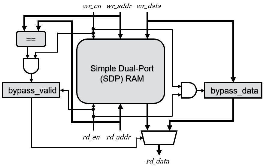
endmoduleThe way I think about implementing write-first behavior is as a “bypass” of the normal RAM read. On line 24, I store the data being written into a bypass register when a read and write happen simultaneously. On line 25, I track whether the bypass register is valid by checking if the read and write addresses match. Notice that deasserting the read enable preserves the bypass register’s contents. While there are other ways to define the read enable, I want the bypass logic to mirror the behavior of a standard RAM read, so I use the read enable to control when the read output is preserved.
The only other change required is on line 35, where I use a multiplexer to select the read data—either directly from the RAM or from the bypass register in the case of a read-during-write.
Architecturally, the write-first logic is structured as follows:
Registered Read Data SDP Template
A common feature in block RAMs is an optional register on the read data output. Unless you’re specifically optimizing for latency, using this registered output is typically a good idea to improve clock frequencies, as the memory read process can introduce significant logic delay. The following template adds this functionality:
module ram_sdp_output_reg #(
    parameter int DATA_WIDTH = 16,
    parameter int ADDR_WIDTH = 10
) (
    input  logic                  clk,
    input  logic                  rd_en,
    input  logic [ADDR_WIDTH-1:0] rd_addr,
    output logic [DATA_WIDTH-1:0] rd_data,
    input  logic                  wr_en,
    input  logic [ADDR_WIDTH-1:0] wr_addr,
    input  logic [DATA_WIDTH-1:0] wr_data
);
    logic [DATA_WIDTH-1:0] ram[2**ADDR_WIDTH];
    logic [DATA_WIDTH-1:0] rd_data_ram;

    always_ff @(posedge clk) begin
        if (wr_en) ram[wr_addr] <= wr_data;
        if (rd_en) rd_data_ram <= ram[rd_addr];
    end

    always_ff @(posedge clk) begin
        if (rd_en) rd_data <= rd_data_ram;
    end
endmodule
One important thing to note is that not all memory resources support a read enable on the read data register. This template will still work on those FPGAs, but synthesis simply won’t pack the register into the RAM primitive. It’s a good idea to verify that resources are being packed as expected. To do this, synthesize the template and check both the resource utilization and the post-synthesis schematic. If synthesis is able to pack the register into the RAM, there should be no additional registers in your design. Conversely, if synthesis can’t pack the register, you’ll see registers in both the resource utilization report and the schematic.
As with the basic template, if you don’t need the read enable, simply connect it to 1 when instantiating the template. This will allow synthesis to remove the enable, and in most cases, the register will be packed within the RAM resource.
General SDP Template
Now, let’s combine all the previously discussed functionality into a single, generalized template that can be configured using parameters. The following template introduces a REG_RD_DATA parameter, which controls whether the read data output is registered, and a WRITE_FIRST parameter, which controls the read-during-write behavior.
// Greg Stitt
// StittHub (www.stitt-hub.com)

module ram_sdp_general #(
    parameter int DATA_WIDTH  = 16,
    parameter int ADDR_WIDTH  = 10,
    parameter bit REG_RD_DATA = 1'b0,
    parameter bit WRITE_FIRST = 1'b0
) (
    input  logic                  clk,
    input  logic                  rd_en,
    input  logic [ADDR_WIDTH-1:0] rd_addr,
    output logic [DATA_WIDTH-1:0] rd_data,
    input  logic                  wr_en,
    input  logic [ADDR_WIDTH-1:0] wr_addr,
    input  logic [DATA_WIDTH-1:0] wr_data
);
    logic [DATA_WIDTH-1:0] ram[2**ADDR_WIDTH];
    logic [DATA_WIDTH-1:0] rd_data_ram;

    // Infer the RAM (always use read-first here)
    always_ff @(posedge clk) begin
        if (wr_en) ram[wr_addr] <= wr_data;
        if (rd_en) rd_data_ram <= ram[rd_addr];
    end

    // Add the manual bypassing logic to support write-first.
    if (WRITE_FIRST) begin : l_write_first
        // We don't have a reset in this template, so we'll make sure the valid
        // register is initialized to 0 after the bitstream is loaded.
        logic bypass_valid_r = 1'b0;
        logic [DATA_WIDTH-1:0] bypass_data_r;

        always_ff @(posedge clk) begin
            if (rd_en && wr_en) bypass_data_r <= wr_data;
            if (rd_en) bypass_valid_r <= wr_en && rd_addr == wr_addr;
        end

        // Add the optional registered read port if requested.
        if (REG_RD_DATA) begin : l_reg_rd_data
            always_ff @(posedge clk) if (rd_en) rd_data <= bypass_valid_r ? bypass_data_r : rd_data_ram;
        end else begin : l_no_reg_rd_data
            assign rd_data = bypass_valid_r ? bypass_data_r : rd_data_ram;
        end
    end else begin : l_read_first
        // Add the optional registered read port if requested.
        if (REG_RD_DATA) begin : l_reg_rd_data
            always_ff @(posedge clk) if (rd_en) rd_data <= rd_data_ram;
        end else begin : l_no_reg_rd_data
            assign rd_data = rd_data_ram;
        end
    end
endmoduleWhile this template offers a highly reusable and largely portable RAM structure, it does have some limitations. Most notably, it doesn’t allow control over which type of RAM resource is used. If you don’t need that level of control, the template will likely work fine for you. However, in cases where you want different logical memories to map to different physical RAM resources, this could be a drawback.
Additionally, the bypassing logic and registered read output could be further customized. Currently, the mux in the bypass logic occurs before the register used for the read data. Unless the synthesis tool retimes the mux to come after the register, the register won’t be packed into the RAM resource. Whether this is an issue depends on the rest of your design. Having the mux before the register prevents packing, which means the register has to be placed outside the RAM, increasing the delay when reading from the RAM. On the other hand, having the mux after the register would add delay to any path using the read data, and would also require an additional register to align the bypass data with the read data register’s output.
There is no optimal, one-size-fits-all solution here. These trade-offs are just one example of how you can customize the design to optimize for specific requirements. There are numerous other parameters you could add to control the architecture, but I opted for a general approach that is widely usable and easy to extend.
Quartus-Specialized SDP Template
The following template demonstrates how to specialize the general SDP template for Quartus and Intel/Altera FPGAs. While this template should also work in Vivado, Vivado has a longstanding bug that requires a workaround, which I’ll address in the next example. Interestingly, the VHDL versions of these templates do not require the Vivado-specific workaround and instead have a single general module that works in Quartus and Vivado.
This Quartus-specific template introduces a STYLE parameter, allowing the user to specify the type of RAM resource for each instance. Refer to the documentation for your specific FPGA to see the different possible values.
To communicate our intention to the synthesis tool, we use the ramstyle attribute, as shown on line 22. By adding this single line, we make the template highly flexible.
// Greg Stitt
// StittHub (www.stitt-hub.com)

module ram_sdp_quartus #(
    parameter int DATA_WIDTH = 16,
    parameter int ADDR_WIDTH = 10,
    parameter bit REG_RD_DATA = 1'b0,
    parameter bit WRITE_FIRST = 1'b0,
    parameter string STYLE = ""
) (
    input  logic                  clk,
    input  logic                  rd_en,
    input  logic [ADDR_WIDTH-1:0] rd_addr,
    output logic [DATA_WIDTH-1:0] rd_data,
    input  logic                  wr_en,
    input  logic [ADDR_WIDTH-1:0] wr_addr,
    input  logic [DATA_WIDTH-1:0] wr_data
);
    // Quartus uses the "ramstyle" attribute to control what type of RAM resource
    // is inferred. The acceptable values vary across FPGAs, but are usually
    // "M4K", "M9K", "M20K", "M144k", and "MLAB".
    (* ramstyle = STYLE *) logic [DATA_WIDTH-1:0] ram[2**ADDR_WIDTH];
    logic [DATA_WIDTH-1:0] rd_data_ram;

    always_ff @(posedge clk) begin
        if (wr_en) ram[wr_addr] <= wr_data;
        if (rd_en) rd_data_ram <= ram[rd_addr];
    end

    if (WRITE_FIRST) begin : l_write_first
        logic bypass_valid_r = 1'b0;
        logic [DATA_WIDTH-1:0] bypass_data_r;

        always_ff @(posedge clk) begin
            if (rd_en && wr_en) bypass_data_r <= wr_data;
            if (rd_en) bypass_valid_r <= wr_en && rd_addr == wr_addr;
        end

        if (REG_RD_DATA) begin : l_reg_rd_data
            always_ff @(posedge clk) if (rd_en) rd_data <= bypass_valid_r ? bypass_data_r : rd_data_ram;
        end else begin : l_no_reg_rd_data
            assign rd_data = bypass_valid_r ? bypass_data_r : rd_data_ram;
        end
    end else begin : l_read_first
        if (REG_RD_DATA) begin : l_reg_rd_data
            always_ff @(posedge clk) if (rd_en) rd_data <= rd_data_ram;
        end else begin : l_no_reg_rd_data
            assign rd_data = rd_data_ram;
        end
    end
endmoduleAs mentioned earlier, Intel/Altera FPGAs often do not provide RAM resources that directly support a read enable. If you don’t require the read enable, simply set it to 1 when instantiating the template. Regardless, the template will still work. If the read enable is needed, Quartus will add extra logic outside the RAM resource to implement the functionality.
Vivado-Specialized SDP Template
The following template demonstrates the workaround required to use the STYLE parameter in Vivado. Ideally, this bug will be fixed in future versions, allowing this template to be merged with the previous one. Or, if this workaround is too annoying, you can use the VHDL version, which works as expected.
The issue with Vivado is that it does not support attributes defined using a string parameter. The ram_style attribute must be a hardcoded string literal. Interestingly, passing the STYLE parameter through $sformat to generate a string works, but unfortunately, most simulators don’t support this method.
The workaround is somewhat clunky, but it’s manageable if you’re only using Vivado. Essentially, you need to use an if-generate block for each possible STYLE value so you can apply a different string literal to the attribute. This introduces another challenge, though. The scope of signals declared within an if-generate block is limited to that block, so we can’t directly use the ram signal elsewhere. Fortunately, SystemVerilog offers a solution: we can reference signals in different scopes by using the label of that scope as a prefix. Instead of just referencing ram, we would use l_ram.ram, where l_ram is the label for the if-generate block.
// Greg Stitt
// StittHub (www.stitt-hub.com)

module ram_sdp_vivado #(
    parameter int DATA_WIDTH = 16,
    parameter int ADDR_WIDTH = 10,
    parameter bit REG_RD_DATA = 1'b0,
    parameter bit WRITE_FIRST = 1'b0,
    parameter string STYLE = ""
) (
    input  logic                  clk,
    input  logic                  rd_en,
    input  logic [ADDR_WIDTH-1:0] rd_addr,
    output logic [DATA_WIDTH-1:0] rd_data,
    input  logic                  wr_en,
    input  logic [ADDR_WIDTH-1:0] wr_addr,
    input  logic [DATA_WIDTH-1:0] wr_data
);
    // Unlike Quartus, Vivado uses ram_style instead of ramstyle.
    // Ideally, we would imitate the previous this previous code:
    //
    //(* ram_style = STYLE *) logic [DATA_WIDTH-1:0] ram[2**ADDR_WIDTH];

    // However, Vivado has a bug preventing string parameters from being
    // used in attributes. So, we can hardcode a string literal, but
    // that doesn't give us the flexibility to support different styles via a
    // parameter.

    // Strangely, the following works in Vivado, but doesn't in most simulators:
    //(* ram_style = $sformatf("%s", STYLE) *) logic [DATA_WIDTH-1:0] ram[2**ADDR_WIDTH];

    // An ugly workaround is to manually specify each possible attribute:
    if (STYLE == "block") begin : l_ram
        (* ram_style = "block" *) logic [DATA_WIDTH-1:0] ram[2**ADDR_WIDTH];
    end else if (STYLE == "distributed") begin : l_ram
        (* ram_style = "distributed" *) logic [DATA_WIDTH-1:0] ram[2**ADDR_WIDTH];
    end else if (STYLE == "registers") begin : l_ram
        (* ram_style = "registers" *) logic [DATA_WIDTH-1:0] ram[2**ADDR_WIDTH];
    end else if (STYLE == "ultra") begin : l_ram
        (* ram_style = "ultra" *) logic [DATA_WIDTH-1:0] ram[2**ADDR_WIDTH];
    end else if (STYLE == "mixed") begin : l_ram
        (* ram_style = "mixed" *) logic [DATA_WIDTH-1:0] ram[2**ADDR_WIDTH];
    end else if (STYLE == "auto") begin : l_ram
        (* ram_style = "auto" *) logic [DATA_WIDTH-1:0] ram[2**ADDR_WIDTH];
    end else if (STYLE == "") begin : l_ram
        logic [DATA_WIDTH-1:0] ram[2**ADDR_WIDTH];
    end else begin : l_ram
        initial begin
            $fatal(1, "Invalid STYLE value %s", STYLE);
        end
    end

    logic [DATA_WIDTH-1:0] rd_data_ram;

    always_ff @(posedge clk) begin
        // To make the earlier workaround work, we need a few small changes here.
        // The ram signal has a scope that's only visible within its if-generate
        // region, so to access it from outside that scope, we need to use a
        // prefix with the generate label l_ram.
        if (wr_en) l_ram.ram[wr_addr] <= wr_data;
        if (rd_en) rd_data_ram <= l_ram.ram[rd_addr];
    end

    if (WRITE_FIRST) begin : l_write_first
        logic bypass_valid_r = 1'b0;
        logic [DATA_WIDTH-1:0] bypass_data_r;

        always_ff @(posedge clk) begin
            if (rd_en && wr_en) bypass_data_r <= wr_data;
            if (rd_en) bypass_valid_r <= wr_en && rd_addr == wr_addr;
        end

        if (REG_RD_DATA) begin : l_reg_rd_data
            always_ff @(posedge clk) if (rd_en) rd_data <= bypass_valid_r ? bypass_data_r : rd_data_ram;
        end else begin : l_no_reg_rd_data
            assign rd_data = bypass_valid_r ? bypass_data_r : rd_data_ram;
        end
    end else begin : l_read_first
        if (REG_RD_DATA) begin : l_reg_rd_data
            always_ff @(posedge clk) if (rd_en) rd_data <= rd_data_ram;
        end else begin : l_no_reg_rd_data
            assign rd_data = rd_data_ram;
        end
    end
endmoduleAdding Resets to the SDP Template
One feature missing from the earlier templates is a reset, which isn’t surprising—most underlying memory resources don’t support reset functionality. However, some of the surrounding logic, such as the bypass register and the read data register, can be reset. The following template shows how to add reset support to the Vivado-specialized version. It’s straightforward to apply the same modification to the other versions as well.
// Greg Stitt
// StittHub (www.stitt-hub.com)

module ram_sdp_with_reset_vivado #(
    parameter int DATA_WIDTH = 16,
    parameter int ADDR_WIDTH = 10,
    parameter bit REG_RD_DATA = 1'b0,
    parameter bit WRITE_FIRST = 1'b0,
    parameter string STYLE = ""
) (
    input logic clk,
    input logic rst,

    input  logic                  rd_en,
    input  logic [ADDR_WIDTH-1:0] rd_addr,
    output logic [DATA_WIDTH-1:0] rd_data,

    input logic                  wr_en,
    input logic [ADDR_WIDTH-1:0] wr_addr,
    input logic [DATA_WIDTH-1:0] wr_data
);
    if (STYLE == "block") begin : l_ram
        (* ram_style = "block" *) logic [DATA_WIDTH-1:0] ram[2**ADDR_WIDTH];
    end else if (STYLE == "distributed") begin : l_ram
        (* ram_style = "distributed" *) logic [DATA_WIDTH-1:0] ram[2**ADDR_WIDTH];
    end else if (STYLE == "registers") begin : l_ram
        (* ram_style = "registers" *) logic [DATA_WIDTH-1:0] ram[2**ADDR_WIDTH];
    end else if (STYLE == "ultra") begin : l_ram
        (* ram_style = "ultra" *) logic [DATA_WIDTH-1:0] ram[2**ADDR_WIDTH];
    end else if (STYLE == "mixed") begin : l_ram
        (* ram_style = "mixed" *) logic [DATA_WIDTH-1:0] ram[2**ADDR_WIDTH];
    end else if (STYLE == "auto") begin : l_ram
        (* ram_style = "auto" *) logic [DATA_WIDTH-1:0] ram[2**ADDR_WIDTH];
    end else if (STYLE == "") begin : l_ram
        logic [DATA_WIDTH-1:0] ram[2**ADDR_WIDTH];
    end else begin : l_ram
        initial begin
            $fatal(1, "Invalid STYLE value %s", STYLE);
        end
    end

    logic [DATA_WIDTH-1:0] rd_data_ram;

    // IMPORTANT: Make sure to not reset anything here or it likely won't be
    // inferred as a RAM.
    always_ff @(posedge clk) begin
        if (wr_en) l_ram.ram[wr_addr] <= wr_data;
        if (rd_en) rd_data_ram <= l_ram.ram[rd_addr];
    end

    if (WRITE_FIRST) begin : l_write_first
        logic bypass_valid_r = 1'b0;
        logic [DATA_WIDTH-1:0] bypass_data_r;

        always_ff @(posedge clk) begin
            if (rd_en && wr_en) bypass_data_r <= wr_data;
            if (rd_en) bypass_valid_r <= wr_en && rd_addr == wr_addr;

            // New reset for the write-first logic.
            if (rst) bypass_valid_r <= 1'b0;
        end

        if (REG_RD_DATA) begin : l_reg_rd_data
            always_ff @(posedge clk) begin
                if (rd_en) rd_data <= bypass_valid_r ? bypass_data_r : rd_data_ram;

                // New reset for the registered read data.
                // IMPORTANT: I would avoid this reset unless absolutely
                // necessary. Just like some FPGAs don't support a read enable
                // on this register, some don't support a reset at all, some
                // only support an async reset, some only support a sync reset,
                // etc. Your design will always still work with this reset, but
                // it may prevent synthesis from packing the register into the
                // RAM resource. You might not care, but when doing timing
                // optimization, you might need to specialize your template for
                // your specific FPGA. You could also go crazy with more
                // if-generate combinations, which is something I have in my
                // personal templates, but I've also been doing this for decades.
                // I don't recommend adding a ton of functionality to your
                // template until you know you are going to use it.
                if (rst) rd_data <= '0;
            end
        end else begin : l_no_reg_rd_data
            assign rd_data = bypass_valid_r ? bypass_data_r : rd_data_ram;
        end
    end else begin : l_read_first
        if (REG_RD_DATA) begin : l_reg_rd_data
            always_ff @(posedge clk) begin
                if (rd_en) rd_data <= rd_data_ram;

                // New reset for the registered read data. See above comment.
                // I avoid this reset whenever possible.
                if (rst) rd_data <= '0;
            end
        end else begin : l_no_reg_rd_data
            assign rd_data = rd_data_ram;
        end
    end
endmoduleThere are a few important considerations when working with resets in memory templates. Most critically, do not apply a reset to any logic related to the RAM array itself or to the core read operation. Doing so may prevent the synthesis tool from inferring a true memory primitive, forcing it to implement the RAM using flip-flops—a highly inefficient outcome that consumes a large number of registers.
For the bypass logic, you can generally reset it however you like, since this logic is almost always implemented outside of the memory block. However, the registered read data output requires more caution. If you want the register to be packed into the RAM resource, you need to choose the type of reset carefully—or possibly omit it entirely. Some FPGAs only support asynchronous resets on this register, others support only synchronous resets, and some do not support any reset at all. While your design will still function if the register is implemented with separate flip-flops, it may come at the cost of extra resources and longer read path delays.
Inferring True Dual-Port (TDP) RAMs
Inferring True Dual-Port (TDP) RAMs is significantly more complex than inferring SDP RAMs, largely because the behavior and supported features of TDP memories vary widely across FPGA families. If you look through the inference templates provided by different vendors, you’ll find substantial differences—not just in syntax, but in behavior. Some memory types, such as UltraRAM in TDP mode, don’t even appear to have complete templates publicly available, at least to the best of my knowledge.
After substantial experimentation, I’ve developed the following templates that work reliably across both AMD/Xilinx and Intel/Altera FPGAs, at least for the device families I tested. These templates intentionally omit certain device-specific features, but they capture the most commonly supported TDP functionality.
Before using any TDP template, it’s critical to understand the exact behavior and constraints of the TDP memory blocks in your target FPGA. For example, some FPGAs do not allow a simultaneous read on one port and write on another port to the same address. Violating these constraints can result in undefined behavior—something that’s easy to miss in simulation but can be catastrophic in hardware.
To mitigate this risk, I strongly recommend adding assertions to these templates that catch invalid or unsafe access patterns for your particular device. These can be conditionally compiled or enabled only during simulation, depending on your verification flow.
General TDP RAM Template
This first template is the most general and portable TDP RAM template I’ve found. The main limitation is that it lacks the STYLE attribute included in earlier SDP templates—but we’ll address that in FPGA-specific versions later on.
One important note: this template does not include a WRITE_FIRST parameter. I’ve intentionally left it out due to the significant variation in read-during-write behavior across FPGA families. For example, the behavior might differ when a read occurs on port A and a write on port B versus the reverse scenario. These behaviors are often hardwired into the memory architecture and can’t always be reliably controlled through inference. Instead, this template focuses on functionality that is most likely to work consistently across all FPGAs.
// Greg Stitt
// StittHub (www.stitt-hub.com)

module ram_tdp #(
    parameter int DATA_WIDTH  = 4,
    parameter int ADDR_WIDTH  = 8,
    parameter bit REG_RD_DATA = 1'b1
) (
    input logic clk,

    // Port A
    input  logic                  en_a,
    input  logic                  wr_en_a,
    input  logic [ADDR_WIDTH-1:0] addr_a,
    input  logic [DATA_WIDTH-1:0] wr_data_a,
    output logic [DATA_WIDTH-1:0] rd_data_a,

    // Port B
    input  logic                  en_b,
    input  logic                  wr_en_b,
    input  logic [ADDR_WIDTH-1:0] addr_b,
    input  logic [DATA_WIDTH-1:0] wr_data_b,
    output logic [DATA_WIDTH-1:0] rd_data_b
);
    logic [DATA_WIDTH-1:0] ram[2**ADDR_WIDTH];
    logic [DATA_WIDTH-1:0] rd_data_ram_a, rd_data_ram_b;

    always @(posedge clk) begin
        if (en_a) begin
            if (wr_en_a) ram[addr_a] <= wr_data_a;
            else rd_data_ram_a <= ram[addr_a];
        end
    end

    always @(posedge clk) begin
        if (en_b) begin
            if (wr_en_b) ram[addr_b] <= wr_data_b;
            else rd_data_ram_b <= ram[addr_b];
        end
    end

    if (REG_RD_DATA) begin : l_reg_rd_data
        always_ff @(posedge clk) begin
            if (en_a) rd_data_a <= rd_data_ram_a;
            if (en_b) rd_data_b <= rd_data_ram_b;
        end
    end else begin : l_no_reg_rd_data
        assign rd_data_a = rd_data_ram_a;
        assign rd_data_b = rd_data_ram_b;
    end
endmodule
The most significant difference from the SDP templates is that TDP RAMs don’t have dedicated read and write ports. Instead, they typically provide two symmetric ports, each capable of both reading and writing. This template models that behavior, requiring the enable signals (en_a and en_b) to be asserted for any memory operation. As noted earlier, TDP memories in Altera FPGAs often don’t natively support this enable signal, but synthesis will still generate the expected behavior by inserting additional logic outside the RAM resource. Alternatively, you can tie the enable signal to 1 during instantiation, in which case synthesis will optimize it away.
Quartus-Specialized TDP RAM Template
In this Quartus-specialized version of the TDP template, we reintroduce the STYLE parameter and apply the ramstyle attribute to specify which type of RAM resource should be used for a given instance. This provides the same flexibility as in the SDP templates. As with earlier examples, this template will also work in Vivado by changing the attribute name from ramstyle to ram_style. However, keep in mind that the same Vivado limitation still applies: the attribute value must be a hardcoded string literal. Again, if you want a unified, generalized template, you could consider the VHDL versions.
// Greg Stitt
// StittHub (www.stitt-hub.com)

module ram_tdp_quartus #(
    parameter int DATA_WIDTH = 4,
    parameter int ADDR_WIDTH = 8,
    parameter bit REG_RD_DATA = 1'b1,
    parameter string STYLE = ""
) (
    input logic clk,

    // Port A
    input  logic                  en_a,
    input  logic                  wr_en_a,
    input  logic [ADDR_WIDTH-1:0] addr_a,
    input  logic [DATA_WIDTH-1:0] wr_data_a,
    output logic [DATA_WIDTH-1:0] rd_data_a,

    // Port B
    input  logic                  en_b,
    input  logic                  wr_en_b,
    input  logic [ADDR_WIDTH-1:0] addr_b,
    input  logic [DATA_WIDTH-1:0] wr_data_b,
    output logic [DATA_WIDTH-1:0] rd_data_b
);
    (* ramstyle = STYLE *) logic [DATA_WIDTH-1:0] ram[2**ADDR_WIDTH];
    logic [DATA_WIDTH-1:0] rd_data_ram_a, rd_data_ram_b;

    always @(posedge clk) begin
        if (en_a) begin
            if (wr_en_a) ram[addr_a] <= wr_data_a;
            else rd_data_ram_a <= ram[addr_a];
        end
    end

    always @(posedge clk) begin
        if (en_b) begin
            if (wr_en_b) ram[addr_b] <= wr_data_b;
            else rd_data_ram_b <= ram[addr_b];
        end
    end

    if (REG_RD_DATA) begin : l_reg_rd_data
        always_ff @(posedge clk) begin
            if (en_a) rd_data_a <= rd_data_ram_a;
            if (en_b) rd_data_b <= rd_data_ram_b;
        end
    end else begin : l_no_reg_rd_data
        assign rd_data_a = rd_data_ram_a;
        assign rd_data_b = rd_data_ram_b;
    end
endmodule
Vivado-Specialized TDP RAM Template
Finally, we can update the TDP template in the same way we modified the SDP template to create a flexible version tailored for Vivado. This allows us to work around the attribute limitation while retaining control over the selected RAM resource.
// Greg Stitt
// StittHub (www.stitt-hub.com)

module ram_tdp_vivado #(
    parameter int DATA_WIDTH = 4,
    parameter int ADDR_WIDTH = 8,
    parameter bit REG_RD_DATA = 1'b1,
    parameter string STYLE = ""
) (
    input logic clk,

    // Port A
    input  logic                  en_a,
    input  logic                  wr_en_a,
    input  logic [ADDR_WIDTH-1:0] addr_a,
    input  logic [DATA_WIDTH-1:0] wr_data_a,
    output logic [DATA_WIDTH-1:0] rd_data_a,

    // Port B
    input  logic                  en_b,
    input  logic                  wr_en_b,
    input  logic [ADDR_WIDTH-1:0] addr_b,
    input  logic [DATA_WIDTH-1:0] wr_data_b,
    output logic [DATA_WIDTH-1:0] rd_data_b
);
    if (STYLE == "block") begin : l_ram
        (* ram_style = "block" *) logic [DATA_WIDTH-1:0] ram[2**ADDR_WIDTH];
    end else if (STYLE == "ultra") begin : l_ram
        (* ram_style = "ultra" *) logic [DATA_WIDTH-1:0] ram[2**ADDR_WIDTH];
    end else if (STYLE == "mixed") begin : l_ram
        (* ram_style = "mixed" *) logic [DATA_WIDTH-1:0] ram[2**ADDR_WIDTH];
    end else if (STYLE == "auto") begin : l_ram
        (* ram_style = "auto" *) logic [DATA_WIDTH-1:0] ram[2**ADDR_WIDTH];
    end else if (STYLE == "") begin : l_ram
        logic [DATA_WIDTH-1:0] ram[2**ADDR_WIDTH];
    end else begin : l_ram
        initial begin
            $fatal(1, "Invalid STYLE value %s", STYLE);
        end
    end

    logic [DATA_WIDTH-1:0] rd_data_ram_a, rd_data_ram_b;

    // BlockRAM can use different clocks on each port, but UltraRAM can't so
    // we use a single clock to support both.
    always @(posedge clk) begin
        if (en_a) begin
            if (wr_en_a) l_ram.ram[addr_a] <= wr_data_a;
            else rd_data_ram_a <= l_ram.ram[addr_a];
        end
    end

    always @(posedge clk) begin
        if (en_b) begin
            if (wr_en_b) l_ram.ram[addr_b] <= wr_data_b;
            else rd_data_ram_b <= l_ram.ram[addr_b];
        end
    end

    if (REG_RD_DATA) begin : l_reg_rd_data
        always_ff @(posedge clk) begin
            if (en_a) rd_data_a <= rd_data_ram_a;
            if (en_b) rd_data_b <= rd_data_ram_b;
        end
    end else begin : l_no_reg_rd_data
        assign rd_data_a = rd_data_ram_a;
        assign rd_data_b = rd_data_ram_b;
    end
endmoduleFinal Thoughts
In this article, I introduced a set of flexible RAM inference templates that cover the most commonly used features across modern FPGAs. While none of them are truly one-size-fits-all, they strike a balance between portability and practical utility, and they can be easily extended to support device-specific capabilities. In over two decades of FPGA design, I’ve only rarely needed to directly instantiate RAM primitives—almost all my designs rely on variations of these templates.
Once you’re comfortable with these patterns, the next step toward mastering FPGA design is understanding how to leverage the low-level features of specific memory resources. RAM inference is a perfect example of how HDL development bridges the gap between behavioral description and hardware implementation. Knowing how your code maps to physical structures isn’t just helpful—it’s essential for writing efficient, scalable, and maintainable designs.
These templates provide a solid foundation. From here, you can adapt and refine them to suit the exact needs of your design and your target FPGA. In a future article, I’ll explore techniques for optimizing logic around memory primitives and offer guidance on when to target different RAM types for best performance and area efficiency.